- 您現在的位置:買賣IC網 > PDF目錄373974 > ADA4899-1YCPZ-R2 (ANALOG DEVICES INC) Unity Gain Stable, Ultralow Distortion, 1 nV/ Hz Voltage Noise, High Speed Op Amp PDF資料下載
參數資料
| 型號: | ADA4899-1YCPZ-R2 |
| 廠商: | ANALOG DEVICES INC |
| 元件分類: | 運動控制電子 |
| 英文描述: | Unity Gain Stable, Ultralow Distortion, 1 nV/ Hz Voltage Noise, High Speed Op Amp |
| 中文描述: | OP-AMP, 230 uV OFFSET-MAX, DSO8 |
| 封裝: | 3 X 3 MM, ROHS COMPLIANT, LFCSP-8 |
| 文件頁數: | 16/20頁 |
| 文件大小: | 496K |
| 代理商: | ADA4899-1YCPZ-R2 |
ADA4899-1
DISABLE PIN OPERATION
Rev. A | Page 16 of 20
The ADA4899-1 DISABLE pin performs three functions:
enable, disable, and reduction of the input bias current. When
the DISABLE pin is brought to within 0.7 V of the positive
supply, the input bias current circuit is enabled. This reduces
the input bias current by a factor of 100. In this state, the input
current noise doubles from 2.6 pA to 5.2 pA/
√
Hz. Table 7
outlines the DISABLE pin operation.
Table 7. DISABLE Pin Truth Table
Supply Voltage
Disable
Enable
Low Input Bias Current
ADA4899-1 MUX
With a true output disable, the ADA4899-1 can be used in
multiplexer applications. The outputs of two ADA4899-1s are
wired together to form a 2:1 mux. Figure 51 shows the 2:1 mux
schematic.
±5 V
5 to +2.4
Open
4.3 to 5
+5 V
0 to 2.4
Open
4.3 to 5
0
0V 1MHz
+5V
–5V
+5V
–5V
0.1μF
0.1μF
ADA4899-1
2V p-p
+5V
–5V
0.1μF
0.1μF
ADA4899-1
0.1μF
2.2μF
0.1μF
2.2μF
+
+
2k
1k
50
1.02k
50
V
REF
= 2.50V
2k
1V p-p
DISABLE
AD8137
DISABLE
50
R
T
50
V
OUT
Figure 51. ADA4899-1 2:1 Mux Schematic
An
AD8137
differential amplifier is used as a level translator
that converts the TTL input to a complementary ±3 V output to
drive the DISABLE pins of the ADA4899-1s. The transient
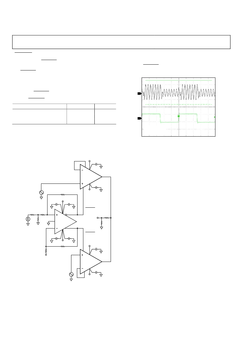
response for the 2:1 mux is shown in Figure 52.
0
2
1
CH1 = 500mV/DIV
CH2 = 5V/DIV
200ns/DIV
Figure 52. ADA4899-1 2:1 Mux Transient Response
CIRCUIT CONSIDERATIONS
Careful and deliberate attention to detail when laying out the
ADA4899-1 board yields optimal performance. Power supply
bypassing, parasitic capacitance, and component selection all
contribute to the overall performance of the amplifier.
PCB Layout
Because the ADA4899-1 can operate up to 600 MHz, it is
essential that RF board layout techniques be employed. All
ground and power planes under the pins of the ADA4899-1
should be cleared of copper to prevent the formation of
parasitic capacitance between the input pins to ground and the
output pins to ground. A single mounting pad on a SOIC
footprint can add as much as 0.2 pF of capacitance to ground if
the ground plane is not cleared from under the mounting pads.
The low distortion pinout of the ADA4899-1 reduces the
distance between the output and the inverting input of the
amplifier. This helps minimize the parasitic inductance and
capacitance of the feedback path, which reduces ringing and
second harmonic distortion.
Power Supply Bypassing
Power supply bypassing for the ADA4899-1 has been optimized
for frequency response and distortion performance. Figure 40
shows the recommended values and location of the bypass
capacitors. Power supply bypassing is critical for stability,
frequency response, distortion, and PSR performance. The
0.1 μF capacitors shown in Figure 40 should be as close to the
supply pins of the ADA4899-1 as possible. The electrolytic
capacitors should be directly adjacent to the 0.1 μF capacitors.
The capacitor between the two supplies helps improve PSR and
distortion performance. In some cases, additional paralleled
capacitors can help improve frequency and transient response.
相關PDF資料 |
PDF描述 |
|---|---|
| ADA4899-1YCPZ-R7 | Unity Gain Stable, Ultralow Distortion, 1 nV/ Hz Voltage Noise, High Speed Op Amp |
| ADA4899-1YCPZ-RL | Unity Gain Stable, Ultralow Distortion, 1 nV/ Hz Voltage Noise, High Speed Op Amp |
| ADA4899-1YRDZ | Unity Gain Stable, Ultralow Distortion, 1 nV/ Hz Voltage Noise, High Speed Op Amp |
| ADA4899-1YRDZ-R7 | Unity Gain Stable, Ultralow Distortion, 1 nV/ Hz Voltage Noise, High Speed Op Amp |
| ADA4899-1YRDZ-RL | Unity Gain Stable, Ultralow Distortion, 1 nV/ Hz Voltage Noise, High Speed Op Amp |
相關代理商/技術參數 |
參數描述 |
|---|---|
| ADA4899-1YCPZ-R7 | 功能描述:IC OPAMP VF ULN ULDIST 8LFCSP RoHS:是 類別:集成電路 (IC) >> Linear - Amplifiers - Instrumentation 系列:- 產品培訓模塊:Differential Circuit Design Techniques for Communication Applications 標準包裝:1 系列:- 放大器類型:RF/IF 差分 電路數:1 輸出類型:差分 轉換速率:9800 V/µs 增益帶寬積:- -3db帶寬:2.9GHz 電流 - 輸入偏壓:3µA 電壓 - 輸入偏移:- 電流 - 電源:40mA 電流 - 輸出 / 通道:- 電壓 - 電源,單路/雙路(±):3 V ~ 3.6 V 工作溫度:-40°C ~ 85°C 安裝類型:表面貼裝 封裝/外殼:16-VQFN 裸露焊盤,CSP 供應商設備封裝:16-LFCSP-VQ 包裝:剪切帶 (CT) 產品目錄頁面:551 (CN2011-ZH PDF) 其它名稱:ADL5561ACPZ-R7CT |
| ADA4899-1YCPZ-RL | 功能描述:IC OPAMP VF ULN ULDIST 8LFCSP RoHS:是 類別:集成電路 (IC) >> Linear - Amplifiers - Instrumentation 系列:- 標準包裝:50 系列:- 放大器類型:通用 電路數:2 輸出類型:滿擺幅 轉換速率:1.8 V/µs 增益帶寬積:6.5MHz -3db帶寬:4.5MHz 電流 - 輸入偏壓:5nA 電壓 - 輸入偏移:100µV 電流 - 電源:65µA 電流 - 輸出 / 通道:35mA 電壓 - 電源,單路/雙路(±):1.8 V ~ 5.25 V,±0.9 V ~ 2.625 V 工作溫度:-40°C ~ 85°C 安裝類型:表面貼裝 封裝/外殼:10-TFSOP,10-MSOP(0.118",3.00mm 寬) 供應商設備封裝:10-MSOP 包裝:管件 |
| ADA4899-1YCPZ-RL7 | 制造商:Analog Devices 功能描述:OP AMP SGL VOLT FDBK 6V/12V 8LFCSP - Tape and Reel |
| ADA4899-1YRD-EBZ | 功能描述:BOARD EVAL FOR ADA4899-1YRD RoHS:是 類別:編程器,開發系統 >> 評估板 - 運算放大器 系列:- 產品培訓模塊:Lead (SnPb) Finish for COTS Obsolescence Mitigation Program 標準包裝:1 系列:- |
| ADA4899-1YRDZ | 功能描述:IC OPAMP VF ULN ULDIST 8SOIC RoHS:是 類別:集成電路 (IC) >> Linear - Amplifiers - Instrumentation 系列:- 標準包裝:2,500 系列:- 放大器類型:通用 電路數:4 輸出類型:- 轉換速率:0.6 V/µs 增益帶寬積:1MHz -3db帶寬:- 電流 - 輸入偏壓:45nA 電壓 - 輸入偏移:2000µV 電流 - 電源:1.4mA 電流 - 輸出 / 通道:40mA 電壓 - 電源,單路/雙路(±):3 V ~ 32 V,±1.5 V ~ 16 V 工作溫度:0°C ~ 70°C 安裝類型:表面貼裝 封裝/外殼:14-TSSOP(0.173",4.40mm 寬) 供應商設備封裝:14-TSSOP 包裝:帶卷 (TR) 其它名稱:LM324ADTBR2G-NDLM324ADTBR2GOSTR |
發布緊急采購,3分鐘左右您將得到回復。