- 您現在的位置:買賣IC網 > PDF目錄373974 > ADA4922-1ARDZ (ANALOG DEVICES INC) High Voltage, Differential 18-Bit ADC Driver PDF資料下載
參數資料
| 型號: | ADA4922-1ARDZ |
| 廠商: | ANALOG DEVICES INC |
| 元件分類: | 運動控制電子 |
| 英文描述: | High Voltage, Differential 18-Bit ADC Driver |
| 中文描述: | OP-AMP, PDSO8 |
| 封裝: | LEAD FREE, MS-012AA, SOIC-8 |
| 文件頁數: | 5/20頁 |
| 文件大小: | 312K |
| 代理商: | ADA4922-1ARDZ |
ADA4922-1
ABSOLUTE MAXIMUM RATINGS
Table 3.
Parameter
Supply Voltage
Power Dissipation
Storage Temperature Range
Operating Temperature Range
Lead Temperature Range (Soldering 10 sec)
Junction Temperature
Rev. 0 | Page 5 of 20
Rating
26 V
See Figure 3
–65°C to +125°C
–40°C to +85°C
300°C
150°C
Stresses above those listed under Absolute Maximum Ratings
may cause permanent damage to the device. This is a stress
rating only; functional operation of the device at these or any
other conditions above those indicated in the operational
section of this specification is not implied. Exposure to absolute
maximum rating conditions for extended periods may affect
device reliability.
THERMAL RESISTANCE
θ
JA
is specified for the worst-case conditions, that is, θ
JA
is
specified for a device soldered in the circuit board with its
exposed paddle soldered to a pad on the PCB surface that is
thermally connected to a copper plane, with zero airflow.
Table 4. Thermal Resistance
Package Type
8-Lead SOIC with EP on 4-layer board
8-Lead LFCSP with EP on 4-layer board
θ
JA
79
81
θ
JC
25
17
Unit
°
C/W
°
C/W
Maximum Power Dissipation
The maximum safe power dissipation in the ADA4922-1
package is limited by the associated rise in junction temperature
(T
J
) on the die. At approximately 150°C, which is the glass
transition temperature, the plastic changes its properties. Even
temporarily exceeding this temperature limit can change the
stresses that the package exerts on the die, permanently shifting
the parametric performance of the ADA4922-1. Exceeding a
junction temperature of 150°C for an extended period can
result in changes in the silicon devices potentially causing
failure.
The power dissipated in the package (P
D
) is the sum of the
quiescent power dissipation and the power dissipated in the
package due to the load drive for all outputs. The quiescent
power is the voltage between the supply pins (V
S
) times the
quiescent current (I
S
). The power dissipated due to the load
drive depends upon the particular application. For each output,
the power due to load drive is calculated by multiplying the load
current by the associated voltage drop across the device. The
power dissipated due to all of the loads is equal to the sum of
the power dissipation due to each individual load. RMS voltages
and currents must be used in these calculations.
Airflow increases heat dissipation, effectively reducing θ
JA
. In
addition, more metal directly in contact with the package leads
from metal traces, through holes, ground, and power planes
reduces the θ
JA
. The exposed paddle on the underside of the
package must be soldered to a pad on the PCB surface that is
thermally connected to a copper plane to achieve the specified θ
JA
.
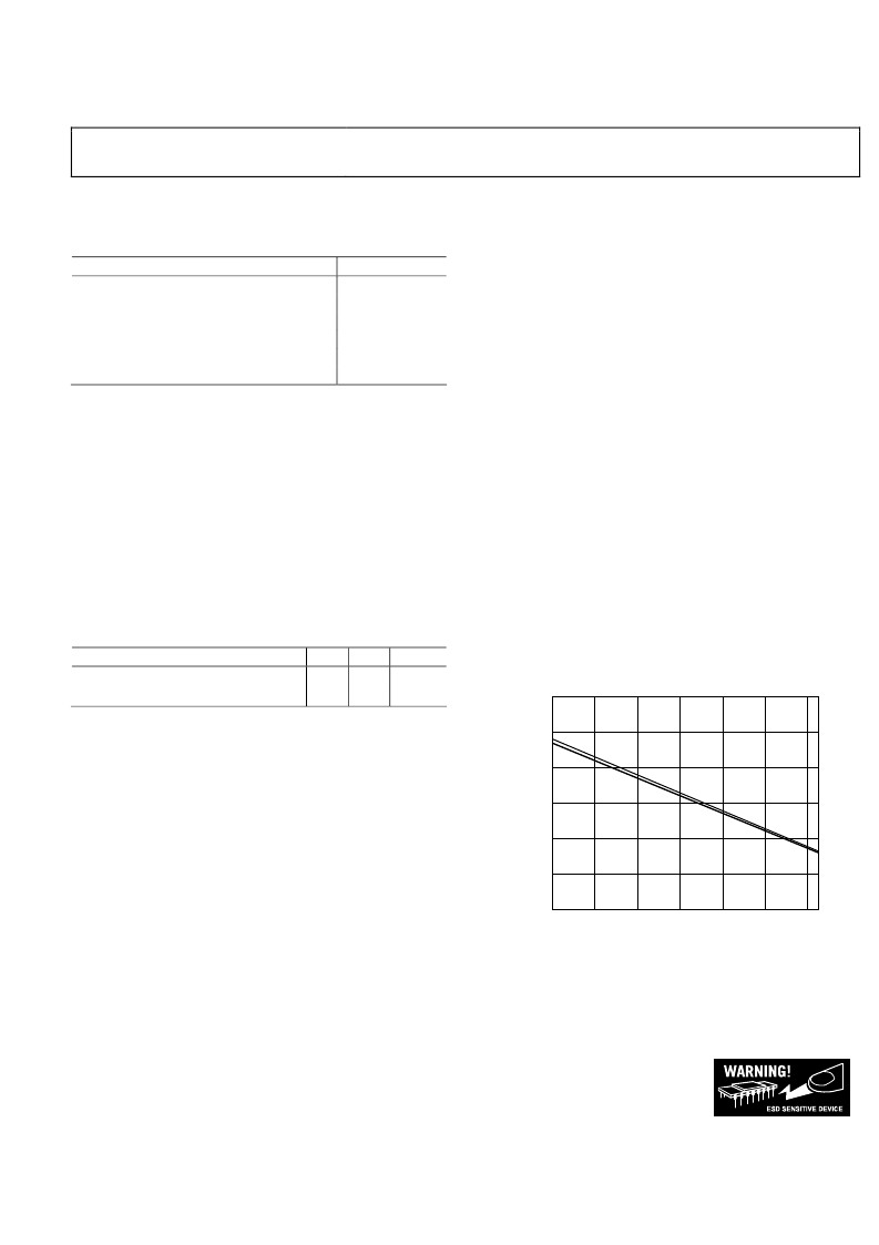
Figure 3 shows the maximum safe power dissipation in the
packages vs. the ambient temperature for the 8-lead SOIC
(79°C/W) and for the 8-lead LFCSP (81°C/W) on a JEDEC
standard 4-layer board, each with its underside paddle soldered
to a pad that is thermally connected to a PCB plane. θ
JA
values
are approximations.
3.0
0
–40
80
0
AMBIENT TEMPERATURE (
°
C)
M
2.5
2.0
1.5
1.0
0.5
–20
0
20
40
60
SOIC
LFCSP
Figure 3. Maximum Power Dissipation vs. Temperature for a 4-Layer Board
ESD CAUTION
ESD (electrostatic discharge) sensitive device. Electrostatic charges as high as 4000 V readily accumulate on
the human body and test equipment and can discharge without detection. Although this product features
proprietary ESD protection circuitry, permanent damage may occur on devices subjected to high energy
electrostatic discharges. Therefore, proper ESD precautions are recommended to avoid performance
degradation or loss of functionality.
相關PDF資料 |
PDF描述 |
|---|---|
| ADA4922-1ARDZ-R7 | High Voltage, Differential 18-Bit ADC Driver |
| ADA4922-1ARDZ-RL | High Voltage, Differential 18-Bit ADC Driver |
| ADA4937-1 | Ultralow Distortion, Differential ADC Driver |
| ADA4937-1_07 | Ultralow Distortion, Differential ADC Driver |
| ADA4937-1YCPZ-R2 | Ultralow Distortion, Differential ADC Driver |
相關代理商/技術參數 |
參數描述 |
|---|---|
| ADA4922-1ARDZ-R7 | 功能描述:IC ADC DRIVER 18BIT DIFF 8-SOIC RoHS:是 類別:集成電路 (IC) >> 線性 - 放大器 - 專用 系列:- 產品培訓模塊:Lead (SnPb) Finish for COTS Obsolescence Mitigation Program 標準包裝:60 系列:- 類型:可變增益放大器 應用:CATV 安裝類型:表面貼裝 封裝/外殼:20-WQFN 裸露焊盤 供應商設備封裝:20-TQFN-EP(5x5) 包裝:托盤 |
| ADA4922-1ARDZ-RL | 功能描述:IC ADC DRIVER 18BIT DIFF 8-SOIC RoHS:是 類別:集成電路 (IC) >> 線性 - 放大器 - 專用 系列:- 產品培訓模塊:Lead (SnPb) Finish for COTS Obsolescence Mitigation Program 標準包裝:60 系列:- 類型:可變增益放大器 應用:CATV 安裝類型:表面貼裝 封裝/外殼:20-WQFN 裸露焊盤 供應商設備封裝:20-TQFN-EP(5x5) 包裝:托盤 |
| ADA4927-1 | 制造商:AD 制造商全稱:Analog Devices 功能描述:Ultralow Distortion Current Feedback Differential ADC Driver |
| ADA4927-1YCP-EBZ | 功能描述:BOARD EVAL FOR ADA4927-1YCP RoHS:是 類別:編程器,開發系統 >> 評估板 - 運算放大器 系列:- 產品培訓模塊:Lead (SnPb) Finish for COTS Obsolescence Mitigation Program 標準包裝:1 系列:- |
| ADA4927-1YCPZ-R2 | 制造商:Analog Devices 功能描述:SP Amp Differential ADC Driver Single 11V 16-Pin LFCSP EP T/R 制造商:Analog Devices 功能描述:SP AMP DIFFERENTIAL ADC DRVR SGL 11V 16LFCSP EP - Tape and Reel 制造商:Analog Devices 功能描述:ANAADA4927-1YCPZ-R2 ULTRALW DISTORTION C 制造商:Analog Devices 功能描述:OP AMP CF DIFF 65MA LN 16LFCSP 制造商:Analog Devices 功能描述:OP AMP, CF, DIFF, 65MA, LN, 16LFCSP 制造商:Analog Devices 功能描述:OP AMP, CF, DIFF, 65MA, LN, 16LFCSP; No. of Amplifiers:1; Input Offset Voltage:1.3mV; Bandwidth:2.3GHz; Amplifier Case Style:LFCSP; No. of Pins:16; Supply Voltage Range:4.5V to 11V; Slew Rate:5000V/s; Supply Current:20mA; Operating ;RoHS Compliant: Yes |
發布緊急采購,3分鐘左右您將得到回復。