- 您現在的位置:買賣IC網 > PDF目錄16955 > ADA4932-1YCP-EBZ (Analog Devices Inc)BOARD EVAL FOR ADA4932-1YCP PDF資料下載
參數資料
| 型號: | ADA4932-1YCP-EBZ |
| 廠商: | Analog Devices Inc |
| 文件頁數: | 1/29頁 |
| 文件大小: | 0K |
| 描述: | BOARD EVAL FOR ADA4932-1YCP |
| 標準包裝: | 1 |
| 每 IC 通道數: | 1 - 單 |
| 放大器類型: | 差分 |
| 板類型: | 裸(未填充) |
| 已供物品: | 板 |
| 已用 IC / 零件: | 16-LFCSP 封裝 |
當前第1頁第2頁第3頁第4頁第5頁第6頁第7頁第8頁第9頁第10頁第11頁第12頁第13頁第14頁第15頁第16頁第17頁第18頁第19頁第20頁第21頁第22頁第23頁第24頁第25頁第26頁第27頁第28頁第29頁
Low Power
Differential ADC Driver
Data Sheet
FEATURES
High performance at low power
High speed
3 dB bandwidth of 560 MHz, G = 1
0.1 dB gain flatness to 300 MHz
Slew rate: 2800 V/s, 25% to 75%
Fast 0.1% settling time of 9 ns
Low power: 9.6 mA per amplifier
Low harmonic distortion
100 dB SFDR at 10 MHz
90 dB SFDR at 20 MHz
Low input voltage noise: 3.6 nV/√Hz
±0.5 mV typical input offset voltage
Externally adjustable gain
Can be used with fractional differential gains
Differential-to-differential or single-ended-to-differential
operation
Adjustable output common-mode voltage
Input common-mode range shifted down by 1 VBE
Wide supply range: +3 V to ±5 V
Available in 16-lead and 24-lead LFCSP packages
APPLICATIONS
ADC drivers
Single-ended-to-differential converters
IF and baseband gain blocks
Differential buffers
Line drivers
GENERAL DESCRIPTION
The ADA4932-x is the next generation AD8132 with higher
performance, and lower noise and power consumption. It is an
ideal choice for driving high performance ADCs as a single-ended-
to-differential or differential-to-differential amplifier. The output
common-mode voltage is user adjustable by means of an internal
common-mode feedback loop, allowing the ADA4932-x output
to match the input of the ADC. The internal feedback loop also
provides exceptional output balance as well as suppression of
even-order harmonic distortion products.
With the ADA4932-x, differential gain configurations are easily
realized with a simple external four-resistor feedback network that
determines the closed-loop gain of the amplifier.
The ADA4932-x is fabricated using the Analog Devices, Inc.,
proprietary silicon-germanium (SiGe) complementary bipolar
process, enabling it to achieve low levels of distortion and noise
at low power consumption. The low offset and excellent dynamic
performance of the ADA4932-x make it well suited for a wide
variety of data acquisition and signal processing applications.
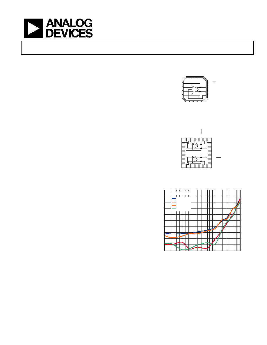
FUNCTIONAL BLOCK DIAGRAMS
1
–FB
2
+IN
3
–IN
4
+FB
11 –OUT
12 PD
10 +OUT
9
VOCM
5
+V
S
6
+V
S
7
+V
S
8
+V
S
15
–V
S
16
–V
S
14
–V
S
13
–V
S
ADA4932-1
07752-
001
Figure 1. ADA4932-1
07752-
002
2
1
3
4
5
6
18
17
16
15
14
13
+IN2
–FB2
+VS1
+FB1
–IN1
–OUT2
PD2
–VS2
VOCM1
+OUT1
8
9
10
11
7
+
F
B2
+V
S2
+V
S2
V
O
CM
2
12
+
OU
T2
–I
N2
20
19
21
P
D1
–O
UT
1
–V
S1
22
–V
S1
23
–F
B1
24
+
IN1
ADA4932-2
Figure 2. ADA4932-2
–140
–130
–120
–110
–100
–90
–80
–70
–60
–50
–40
100k
1M
10M
100M
HARM
O
NI
C
DI
S
T
O
RT
IO
N
(
d
Bc)
FREQUENCY (Hz)
VOUT, dm = 2V p-p
07752-
003
HD2, G = 1
HD3, G = 1
HD2, G = 2
HD3, G = 2
Figure 3. Harmonic Distortion vs. Frequency at Various Gains
The ADA4932-x is available in a Pb-free, 3 mm × 3 mm 16-lead
LFCSP (ADA4932-1, single) or a Pb-free, 4 mm × 4 mm 24-lead
LFCSP (ADA4932-2, dual). The pinout has been optimized to
facilitate PCB layout and minimize distortion. The ADA4932-1
and the ADA4932-2 are specified to operate over the 40°C to
+105°C temperature range; both operate on supplies between
+3 V and ±5 V.
Rev. C
Information furnished by Analog Devices is believed to be accurate and reliable. However, no
responsibilityisassumedbyAnalogDevicesforitsuse,norforanyinfringementsofpatentsorother
rightsofthirdpartiesthatmayresultfromitsuse.Specificationssubjecttochangewithoutnotice.No
license is granted by implication or otherwise under any patent or patent rights of Analog Devices.
Trademarksandregisteredtrademarksarethepropertyoftheirrespectiveowners.
One Technology Way, P.O. Box 9106, Norwood, MA 02062-9106, U.S.A.
Tel: 781.329.4700
2008–2014 Analog Devices, Inc. All rights reserved.
相關PDF資料 |
PDF描述 |
|---|---|
| ADA4950-1YCP-EBZ | BOARD EVAL FOR ADA4950-1YCP |
| LLS2W221MELC | CAP ALUM 220UF 450V 20% SNAP |
| 222D132-4-60/42-0 | BOOT MOLDED |
| ECM18DRKI-S13 | CONN EDGECARD 36POS .156 EXTEND |
| 222D132-3-60/42-0 | BOOT MOLDED |
相關代理商/技術參數 |
參數描述 |
|---|---|
| ADA4932-1YCPZ-R2 | 制造商:Analog Devices 功能描述:SP Amp DIFF AMP Single 制造商:Analog Devices 功能描述:LW CST/LW PWR DIFF ADC DRIVER - Tape and Reel 制造商:Analog Devices 功能描述:ANAADA4932-1YCPZ-R2 LW CST/LW PWR DIFF A 制造商:Analog Devices 功能描述:AMP DIFF LP 80MA 16LFCSP 制造商:Analog Devices 功能描述:AMP, DIFF, LP, 80MA, 16LFCSP 制造商:Analog Devices 功能描述:AMP, DIFF, LP, 80MA, 16LFCSP; No. of Amplifiers:1; Input Offset Voltage:2.2mV; Bandwidth:560MHz; Amplifier Case Style:LFCSP; No. of Pins:16; Supply Voltage Range:3V to 11V; Slew Rate:2800V/s; Supply Current:9.6mA; Operating ;RoHS Compliant: Yes 制造商:Analog Devices 功能描述:SP Amp Diff ADC Driver Single 5.5V/11V |
| ADA4932-1YCPZ-R2 | 制造商:Analog Devices 功能描述:IC DIFF AMP 560MHZ 2800V/ LFCSP-16 |
| ADA4932-1YCPZ-R21 | 制造商:AD 制造商全稱:Analog Devices 功能描述:Low Power Differential ADC Driver |
| ADA4932-1YCPZ-R7 | 功能描述:IC AMP DIFF LP 80MA 16LFCSP RoHS:是 類別:集成電路 (IC) >> Linear - Amplifiers - Instrumentation 系列:- 產品培訓模塊:Differential Circuit Design Techniques for Communication Applications 標準包裝:1 系列:- 放大器類型:RF/IF 差分 電路數:1 輸出類型:差分 轉換速率:9800 V/µs 增益帶寬積:- -3db帶寬:2.9GHz 電流 - 輸入偏壓:3µA 電壓 - 輸入偏移:- 電流 - 電源:40mA 電流 - 輸出 / 通道:- 電壓 - 電源,單路/雙路(±):3 V ~ 3.6 V 工作溫度:-40°C ~ 85°C 安裝類型:表面貼裝 封裝/外殼:16-VQFN 裸露焊盤,CSP 供應商設備封裝:16-LFCSP-VQ 包裝:剪切帶 (CT) 產品目錄頁面:551 (CN2011-ZH PDF) 其它名稱:ADL5561ACPZ-R7CT |
| ADA4932-1YCPZ-R71 | 制造商:AD 制造商全稱:Analog Devices 功能描述:Low Power Differential ADC Driver |
發布緊急采購,3分鐘左右您將得到回復。