- 您現在的位置:買賣IC網 > PDF目錄16927 > ADA4941-1YR-EBZ (Analog Devices Inc)BOARD EVAL FOR ADA4941-1YR PDF資料下載
參數資料
| 型號: | ADA4941-1YR-EBZ |
| 廠商: | Analog Devices Inc |
| 文件頁數: | 1/24頁 |
| 文件大小: | 0K |
| 描述: | BOARD EVAL FOR ADA4941-1YR |
| 標準包裝: | 1 |
| 每 IC 通道數: | 1 - 單 |
| 放大器類型: | 差分 |
| 板類型: | 裸(未填充) |
| 已供物品: | 板 |
| 已用 IC / 零件: | 8-SOIC 封裝 |
Ultralow Distortion
Differential ADC Driver
ADA4939-1/ADA4939-2
Rev. 0
Information furnished by Analog Devices is believed to be accurate and reliable. However, no
responsibilityis assumedbyAnalogDevicesforitsuse,norforanyinfringements of patents or other
rightsofthirdpartiesthatmayresultfromitsuse.Specificationssubjecttochangewithoutnotice.No
license is granted by implication or otherwise under any patent or patent rights of Analog Devices.
Trademarksandregisteredtrademarksarethepropertyoftheirrespectiveowners.
One Technology Way, P.O. Box 9106, Norwood, MA 02062-9106, U.S.A.
Tel: 781.329.4700
www.analog.com
Fax: 781.461.3113
2008 Analog Devices, Inc. All rights reserved.
FEATURES
Extremely low harmonic distortion
102 dBc HD2 @ 10 MHz
83 dBc HD2 @ 70 MHz
77 dBc HD2 @ 100 MHz
101 dBc HD3 @ 10 MHz
97 dBc HD3 @ 70 MHz
91 dBc HD3 @ 100 MHz
Low input voltage noise: 2.3 nV/√Hz
High speed
3 dB bandwidth of 1.4 GHz, G = 2
Slew rate: 6800 V/μs, 25% to 75%
Fast overdrive recovery of <1 ns
±0.5 mV typical offset voltage
Externally adjustable gain
Stable for differential gains ≥2
Differential-to-differential or single-ended-to-differential
operation
Adjustable output common-mode voltage
Single-supply operation: 3.3 V to 5 V
APPLICATIONS
ADC drivers
Single-ended-to-differential converters
IF and baseband gain blocks
Differential buffers
Line drivers
GENERAL DESCRIPTION
The ADA4939 is a low noise, ultralow distortion, high speed
differential amplifier. It is an ideal choice for driving high
performance ADCs with resolutions up to 16 bits from dc to
100 MHz. The output common-mode voltage is user adjustable
by means of an internal common-mode feedback loop, allowing
the ADA4939 output to match the input of the ADC. The internal
feedback loop also provides exceptional output balance as well as
suppression of even-order harmonic distortion products.
With the ADA4939, differential gain configurations are easily
realized with a simple external feedback network of four resistors
that determine the closed-loop gain of the amplifier.
The ADA4939 is fabricated using Analog Devices, Inc., proprietary
silicon-germanium (SiGe), complementary bipolar process,
enabling it to achieve very low levels of distortion with an input
voltage noise of only 2.3 nV/√Hz. The low dc offset and excellent
dynamic performance of the ADA4939 make it well suited for a
wide variety of data acquisition and signal processing applications.
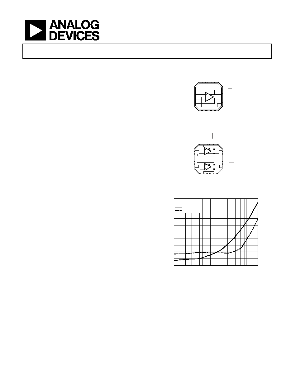
FUNCTIONAL BLOCK DIAGRAMS
1
–FB
2
+IN
3
–IN
4
+FB
11 –OUT
12 PD
10 +OUT
9VOCM
5
+
V
S
6
+
V
S
7
+
V
S
8
+
V
S
15
–V
S
16
–V
S
14
–V
S
13
–V
S
ADA4939-1
074
29
-00
1
Figure 1. ADA4939-1
ADA4939-2
1
–IN1
2
+FB1
3
+VS1
4
+VS1
5
–FB2
6
+IN2
15 –VS2
16 –VS2
17 VOCM1
18 +OUT1
14 PD2
13 –OUT2
7
–I
N
2
8
+
F
B
2
9
+
V
S
2
11
V
O
C
M
2
12
+
O
U
T
2
10
+
V
S
2
21
–V
S
1
22
–V
S
1
23
–
F
B
1
24
+
IN
1
20
P
D
1
19
–O
U
T
1
07
42
9-
0
02
Figure 2. ADA4939-2
–60
–110
–105
–100
–95
–90
–85
–80
–75
–70
–65
1
10
100
HAR
M
O
NI
C
DI
S
T
O
RT
IO
N
(
d
Bc)
FREQUENCY (MHz)
HD2
HD3
VOUT, dm = 2V p-p
07
42
9-
0
21
Figure 3. Harmonic Distortion vs. Frequency
The ADA4939 is available in a Pb-free, 3 mm × 3 mm 16-lead
LFCSP (ADA4939-1, single) or a Pb-free, 4 mm × 4 mm 24-lead
LFCSP (ADA4939-2, dual). The pinout has been optimized to
facilitate PCB layout and minimize distortion. The ADA4939-1
and the ADA4939-2 are specified to operate over the 40°C to
+105°C temperature range; both operate on supplies between
3.3 V and 5 V.
相關PDF資料 |
PDF描述 |
|---|---|
| ADA4939-2YCP-EBZ | BOARD EVAL FOR ADA4939-2YCP |
| ADA4941-1YCP-EBZ | BOARD EVAL FOR ADA4941-1YCP |
| ADA4938-1YCP-EBZ | BOARD EVAL FOR ADA4938-1YCP |
| ADA4939-1YCP-EBZ | BOARD EVAL FOR ADA4939-1YCP |
| 4-1589788-9 | WDUALOBE CONNECTOR |
相關代理商/技術參數 |
參數描述 |
|---|---|
| ADA4941-1YRZ | 功能描述:IC DIFF ADC DVR 18BIT 8-SOIC RoHS:是 類別:集成電路 (IC) >> 線性 - 放大器 - 專用 系列:- 產品培訓模塊:Lead (SnPb) Finish for COTS Obsolescence Mitigation Program 標準包裝:60 系列:- 類型:可變增益放大器 應用:CATV 安裝類型:表面貼裝 封裝/外殼:20-WQFN 裸露焊盤 供應商設備封裝:20-TQFN-EP(5x5) 包裝:托盤 |
| ADA4941-1YRZ-R7 | 功能描述:IC DIFF ADC DRIVER 18BIT 8SOIC RoHS:是 類別:集成電路 (IC) >> 線性 - 放大器 - 專用 系列:- 產品培訓模塊:Lead (SnPb) Finish for COTS Obsolescence Mitigation Program 標準包裝:60 系列:- 類型:可變增益放大器 應用:CATV 安裝類型:表面貼裝 封裝/外殼:20-WQFN 裸露焊盤 供應商設備封裝:20-TQFN-EP(5x5) 包裝:托盤 |
| ADA4941-1YRZ-RL | 功能描述:IC DIFF ADC DRIVER 18BIT 8SOIC RoHS:是 類別:集成電路 (IC) >> 線性 - 放大器 - 專用 系列:- 產品培訓模塊:Lead (SnPb) Finish for COTS Obsolescence Mitigation Program 標準包裝:60 系列:- 類型:可變增益放大器 應用:CATV 安裝類型:表面貼裝 封裝/外殼:20-WQFN 裸露焊盤 供應商設備封裝:20-TQFN-EP(5x5) 包裝:托盤 |
| ADA4950-1 | 制造商:AD 制造商全稱:Analog Devices 功能描述:Low Power, Selectable Gain Differential ADC Driver, G = 1, 2, 3 |
| ADA4950-1YCP-EBZ | 功能描述:BOARD EVAL FOR ADA4950-1YCP RoHS:是 類別:編程器,開發系統 >> 評估板 - 運算放大器 系列:- 產品培訓模塊:Lead (SnPb) Finish for COTS Obsolescence Mitigation Program 標準包裝:1 系列:- |
發布緊急采購,3分鐘左右您將得到回復。