- 您現在的位置:買賣IC網 > PDF目錄373975 > ADCMP341YRJZ-REEL7 (ANALOG DEVICES INC) Dual 0.275% Comparators and Reference with Programmable Hysteresis PDF資料下載
參數資料
| 型號: | ADCMP341YRJZ-REEL7 |
| 廠商: | ANALOG DEVICES INC |
| 元件分類: | 運動控制電子 |
| 英文描述: | Dual 0.275% Comparators and Reference with Programmable Hysteresis |
| 中文描述: | DUAL COMPARATOR, 8000 ns RESPONSE TIME, PDSO8 |
| 封裝: | LEAD FREE, MO-178BA, SOT-23, 8 PIN |
| 文件頁數: | 10/12頁 |
| 文件大小: | 300K |
| 代理商: | ADCMP341YRJZ-REEL7 |
ADCMP341/ADCMP343
APPLICATION INFORMATION
The ADCMP341/ADCMP343 are dual, low power comparators
with a built-in 400 mV reference that operates from 1.7 V to 5.5 V.
The comparators are 0.275% accurate with fully programmable
hysteresis, implemented using a new technique of a three-resistor
string on the input. These open-drain outputs are capable of
sinking up to 40 mA.
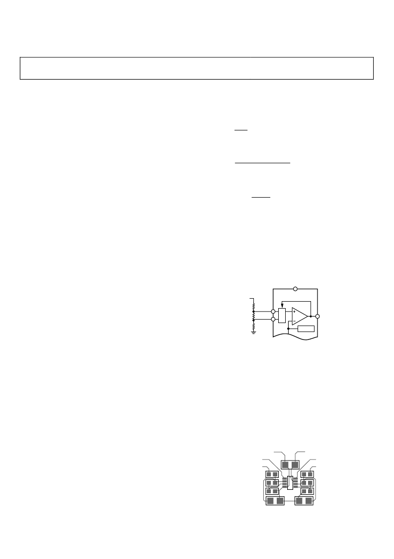
COMPARATORS AND INTERNAL REFERENCE
Each of the comparators has one input available externally; the
other comparator inputs are connected internally to the 400 mV
reference. The ADCMP341 has two noninverting comparators
and the ADCMP343 has two inverting comparators.
There are two input pins available to each comparator. However,
these two input pins (±INx_U, ±INx_L) connect to the same
input leg of the comparator via a muxing system. This is to
provide fully programmable rising and falling trip points. The
output of the comparator determines which pin is connected to
the input of the same comparator. Using Figure 28 as an
example, when OUTA is high, +INA_U is connected to the
comparator input. When the input voltage drops and passes
below the 400 mV reference, the output goes low. This in turn
disconnects +INA_U from the comparator and connects
+INA_L. This leg of the string is at a lower voltage and thus
instantaneously the effect of hysteresis is applied. Therefore,
using a resistor string on the input as shown in Figure 28, the
voltages for the rising and falling trip points can be programmed
by selecting the appropriate resistors in the string.
POWER SUPPLY
The ADCMP341/ADCMP343 are designed to operate from 1.7 V
to 5.5 V A 0.1 μF decoupling capacitor is recommended between
V
DD
and GND.
INPUTS
The comparator inputs are limited to the maximum V
DD
voltage
range. The voltage on these inputs can be above V
DD
but never
above the maximum allowed V
DD
voltage.
OUTPUTS
The open-drain comparator outputs are limited to the maximum
specified V
DD
voltage range, regardless of the V
DD
voltage. These
outputs are capable of sinking up to 40 mA. Outputs can be tied
together to provide a common output signal.
PROGRAMMING HYSTERESIS
When choosing the resistor values, the input bias current must
be considered as a potential source of error. Begin by choosing a
resistor value for R3, which takes into account the acceptable
error introduced by the maximum specified input bias current.
To reduce this error, the current flowing through the Resistor R3
should be considerably greater than the input bias current.
Rev. 0 | Page 10 of 12
BIAS
R3
I
I
>>
R3 is therefore
3
3
R
REF
I
V
R
=
Now R2 can be calculated from the following:
(
RISING
V
)
FALLING
FALLING
V
V
R
R
=
3
2
R1 can then be calculated using the following equation:
2
1
3
1
R
V
V
R
R
REF
RISING
×
=
where:
V
REF
is the specified on chip reference.
I
BIAS
is the maximum specified input bias current.
R1
,
R2,
and
R3
are the three resistors as shown in Figure 28.
I
R3
is the current flowing through
R3
.
V
FALLING
is the desired falling trip voltage and lower of the two.
V
RISING
is the desired rising trip voltage and higher of the two.
+INA_U
OUTA
M
V
DD
400mV
ADCMP341
+INA_L
VINA
R1
R2
R3
0
Figure 28. Programming Hysteresis Example
LAYOUT RECOMMENDATIONS
Correct layout is very important to increase noise immunity.
Long tracks from the input resistors to the device can lead to
noise being coupled onto the inputs. To avoid this, it is best to
place the input resistors as close as possible to the device. It is
also recommended that a GND plane is used under this layout.
The combination of small hysteresis and the use of a large R3
resistor further increases susceptibility to noise. In this case, a
decoupling capacitor (CA, CB) may be required on the ±INx_U
node to help reduce any noise. A recommended layout example
can be seen in Figure 29.
C1
CA
CB
U1
GND
V
DD
OUTA
INA
R1A
R2A
R3A
OUTB
INB
R1B
R2B
R3B
0
Figure 29. Recommended Layout Example
相關PDF資料 |
PDF描述 |
|---|---|
| ADCMP343 | Dual 0.275% Comparators and Reference with Programmable Hysteresis |
| ADCMP343YRJZ-REEL7 | Dual 0.275% Comparators and Reference with Programmable Hysteresis |
| ADCMP350YKS-REEL | Comparators and Reference Circuits |
| ADCMP352YKS-REEL | Comparators and Reference Circuits |
| ADCMP354YKS-REEL | Comparators and Reference Circuits |
相關代理商/技術參數 |
參數描述 |
|---|---|
| ADCMP343 | 制造商:AD 制造商全稱:Analog Devices 功能描述:Dual 0.275% Comparators and Reference with Programmable Hysteresis |
| ADCMP343ARJ | 制造商:AD 制造商全稱:Analog Devices 功能描述:Dual Comparators with 400mV Reference and programmable Hysteresis |
| ADCMP343YRJZ-REEL7 | 功能描述:IC COMPARATOR DUAL OD SOT23-8 RoHS:是 類別:集成電路 (IC) >> 線性 - 比較器 系列:- 標準包裝:25 系列:- 類型:帶電壓基準 元件數:4 輸出類型:CMOS,開路漏極,TTL 電壓 - 電源,單路/雙路(±):2 V ~ 11 V,±1 V ~ 5.5 V 電壓 - 輸入偏移(最小值):10mV @ 5V 電流 - 輸入偏壓(最小值):- 電流 - 輸出(標準):0.015mA @ 5V 電流 - 靜態(最大值):8.5µA CMRR, PSRR(標準):80dB CMRR,80dB PSRR 傳輸延遲(最大):12µs 磁滯:50mV 工作溫度:0°C ~ 70°C 封裝/外殼:16-DIP(0.300",7.62mm) 安裝類型:通孔 包裝:管件 |
| ADCMP343YRJZ-REEL7 | 制造商:Analog Devices 功能描述:IC GEN PUR COMP DUAL 8S SOT-23-8 |
| ADCMP350 | 制造商:AD 制造商全稱:Analog Devices 功能描述:Comparator and Reference Circuits |
發布緊急采購,3分鐘左右您將得到回復。