- 您現(xiàn)在的位置:買(mǎi)賣(mài)IC網(wǎng) > PDF目錄373977 > ADCMP573BCP (ANALOG DEVICES INC) Ultrafast 3.3 V Single-Supply Comparators PDF資料下載
參數(shù)資料
| 型號(hào): | ADCMP573BCP |
| 廠商: | ANALOG DEVICES INC |
| 元件分類(lèi): | 運(yùn)動(dòng)控制電子 |
| 英文描述: | Ultrafast 3.3 V Single-Supply Comparators |
| 中文描述: | COMPARATOR, 5000 uV OFFSET-MAX, QCC16 |
| 封裝: | MO-220-VEED-2, LFCSP-16 |
| 文件頁(yè)數(shù): | 9/16頁(yè) |
| 文件大小: | 412K |
| 代理商: | ADCMP573BCP |
第1頁(yè)第2頁(yè)第3頁(yè)第4頁(yè)第5頁(yè)第6頁(yè)第7頁(yè)第8頁(yè)當(dāng)前第9頁(yè)第10頁(yè)第11頁(yè)第12頁(yè)第13頁(yè)第14頁(yè)第15頁(yè)第16頁(yè)
Preliminary Technical Data
ADCMP572/ADCMP573
APPLICATION INFORMATION
POWER/GROUND LAYOUT AND BYPASSING
The ADCMP572/ADCMP573 comparators are very high speed
SiGe devices. Consequently, it is essential to use proper high
speed design techniques to achieve the specified performance.
Of critical importance is the use of low impedance supply
planes, particularly the output supply plane (V
CCO
) and the
ground plane (GND). Individual supply planes are recom-
mended as part of a multilayer board. Providing the lowest
inductance return path for switching currents ensures the best
possible performance in the target application.
Rev. PrB | Page 9 of 16
It is also important to adequately bypass the input and output
supplies. A 1 μF electrolytic bypass capacitor should be placed
within several inches of each power supply pin to ground. In
addition, multiple high quality 0.1 μF bypass capacitors should
be placed as close as possible to each of the V
CCI
and V
CCO
supply pins and should be connected to the GND plane with
redundant vias. High frequency bypass capacitors should be
carefully selected for minimum inductance and ESR. Parasitic
layout inductance should also be strictly avoided to maximize
the effectiveness of the bypass at high frequencies.
If the input and output supplies are connected separately such
that V
CCI
≠
V
CCO
, then care should be taken to bypass each of
these supplies separately to the GND plane. A bypass capacitor
should not be connected between them. It is recommended that
the GND plane separate the V
CCI
and V
CCO
planes when the
circuit board layout is designed to minimize coupling between
the two supplies and to take advantage of the additional bypass
capacitance from each respective supply to the ground plane.
This enhances the performance when split input/output supplies
are used. If the input and output supplies are connected
together for single-supply operation such that V
CCI
= V
CCO
, then
coupling between the two supplies is unavoidable; however,
every effort should be made to keep the supply plane adjacent
to the GND plane to maximize the additional bypass capacitance
this arrangement provides.
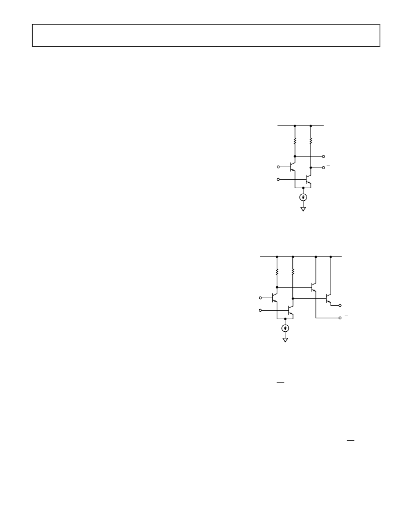
CML/RSPECL OUTPUT STAGE
Specified propagation delay dispersion performance can be
achieved only by using proper transmission line terminations.
The outputs of the ADCMP572 are designed to directly drive
400 mV into 50 cable or microstrip and/or stripline transmis-
sion lines properly terminated to the V
CCO
supply plane. The
CML output stage is shown in the simplified schematic diagram
of Figure 12. The outputs are each back-terminated with 50
for best transmission line matching. The RSPECL outputs of the
ADCMP573 are illustrated in Figure 13 and should be terminated
to V
CCO
2 V. As an alternative, Thevenin equivalent termina-
tion networks may also be used in either case if the direct
termination voltage is not readily available. If high speed output
signals must be routed more than a centimeter, microstrip or
stripline techniques are essential to ensure proper transition
times and to prevent output ringing and pulse-width dependant
propagation delay dispersion. For the most timing critical
applications where transmission line reflections pose the
greatest risk to performance, the ADCMP572 provides the best
match to 50 output transmission paths.
Q
16mA
50
Q
0
V
CCO
GND
Figure 12. Simplified Schematic Diagram of
the ADCMP572 CML Output Stage
0
V
CCO
GND
Q
Q
Figure 13. Simplified Schematic Diagram of
the ADCMP573 RSPECL Output Stage
USING/DISABLING THE LATCH FEATURE
The latch inputs (LE/LE) are active low for latch mode, and are
internally terminated with 50 resistors to Pin 8. This
corresponds to the V
CCO
supply for the ADCMP572 and the V
TT
pin for the ADCMP573. All V
CCO
pins should be connected to
the supply plane for maximum performance, and the V
TT
pin
should be connected externally to V
CCO
– 2 V, preferably to its
own low inductance plane. When using the ADCMP572, the
latch function can be disabled by connecting the LE pin to
GND with an external pull-down resistor and leaving the LE
pin unconnected. To prevent excessive power dissipation, the
resistor should be 750 when V
CCO
= 3.3 V, and 1.2 k when
V
CCO
= 5.2 V. When using the ADCMP573 comparator, the latch
can be disabled by connecting the LE pin to V
CCO
with an
相關(guān)PDF資料 |
PDF描述 |
|---|---|
| ADCMP580 | Ultrafast SiGe Voltage Comparators |
| ADCMP580_05 | Ultrafast SiGe Voltage Comparators |
| ADCMP580BCP-R2 | Ultrafast SiGe Voltage Comparators |
| ADCMP580BCP-RL7 | Ultrafast SiGe Voltage Comparators |
| ADCMP580BCP-WP | Ultrafast SiGe Voltage Comparators |
相關(guān)代理商/技術(shù)參數(shù) |
參數(shù)描述 |
|---|---|
| ADCMP573BCP-R2 | 制造商:Rochester Electronics LLC 功能描述: 制造商:Analog Devices 功能描述: |
| ADCMP573BCPRL7 | 制造商:AD 功能描述:NEW |
| ADCMP573BCP-RL7 | 制造商:Analog Devices 功能描述:Comparator Single 5.4V 16-Pin LFCSP EP T/R |
| ADCMP573BCP-WP | 制造商:Rochester Electronics LLC 功能描述: 制造商:Analog Devices 功能描述:Single Supply, PECL on XFCB3.0-WAFFLE PA |
| ADCMP573BCPZ-R2 | 功能描述:IC COMPARATOR PECL 3.3-5 16LFCSP RoHS:是 類(lèi)別:集成電路 (IC) >> 線性 - 比較器 系列:- 標(biāo)準(zhǔn)包裝:1 系列:- 類(lèi)型:通用 元件數(shù):1 輸出類(lèi)型:CMOS,開(kāi)路集電極,TTL 電壓 - 電源,單路/雙路(±):2.7 V ~ 5.5 V 電壓 - 輸入偏移(最小值):7mV @ 5V 電流 - 輸入偏壓(最小值):0.25µA @ 5V 電流 - 輸出(標(biāo)準(zhǔn)):84mA @ 5V 電流 - 靜態(tài)(最大值):120µA CMRR, PSRR(標(biāo)準(zhǔn)):- 傳輸延遲(最大):600ns 磁滯:- 工作溫度:-40°C ~ 85°C 封裝/外殼:SC-74A,SOT-753 安裝類(lèi)型:表面貼裝 包裝:剪切帶 (CT) 產(chǎn)品目錄頁(yè)面:1268 (CN2011-ZH PDF) 其它名稱:*LMV331M5*LMV331M5/NOPBLMV331M5CT |
發(fā)布緊急采購(gòu),3分鐘左右您將得到回復(fù)。