- 您現(xiàn)在的位置:買賣IC網(wǎng) > PDF目錄373977 > ADCMP582BCP-R2 (ANALOG DEVICES INC) Ultrafast SiGe Voltage Comparators PDF資料下載
參數(shù)資料
| 型號: | ADCMP582BCP-R2 |
| 廠商: | ANALOG DEVICES INC |
| 元件分類: | 運(yùn)動(dòng)控制電子 |
| 英文描述: | Ultrafast SiGe Voltage Comparators |
| 中文描述: | COMPARATOR, 10000 uV OFFSET-MAX, 0.18 ns RESPONSE TIME, QCC16 |
| 封裝: | 3 X 3 MM, MO-220VEED-2, LFCSP-16 |
| 文件頁數(shù): | 7/16頁 |
| 文件大小: | 284K |
| 代理商: | ADCMP582BCP-R2 |
ADCMP580/ADCMP581/ADCMP582
PIN CONFIGURATIONS AND FUNCTION DESCRIPTIONS
Rev. 0 | Page 7 of 16
Q
GND
L
PIN 1
INDICATOR
1
2
3
4
V
TP
V
P
V
N
V
TN
11 Q
10
9
12 GND
5
V
C
6
7
L
8
V
T
1
1
C
1
1
E
ADCMP580
TOP VIEW
(Not to Scale)
0
0
Q
GND
L
PIN 1
INDICATOR
1
2
3
4
V
TP
V
P
V
N
V
TN
11 Q
10
9
12 GND
5
V
C
6
7
L
8
V
T
1
1
C
1
1
E
ADCMP581
TOP VIEW
(Not to Scale)
0
Q
V
CCO
L
PIN 1
INDICATOR
1
2
3
4
V
TP
V
P
V
N
V
TN
11 Q
10
9
12 V
CCO
5
V
C
6
7
L
8
V
T
1
1
C
1
1
E
ADCMP582
TOP VIEW
(Not to Scale)
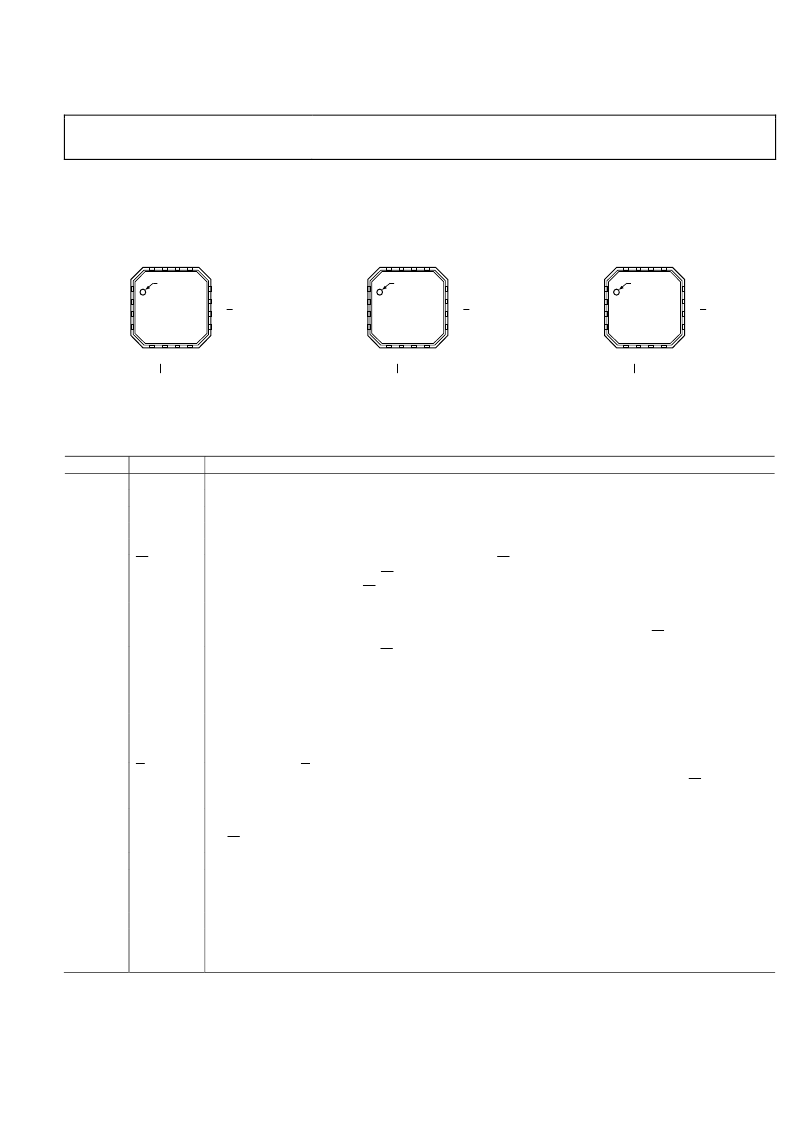
Figure 3. ADCMP580 Pin Configuration
Figure 4. ADCMP581 Pin Configuration
Figure 5. ADCMP582 Pin Configuration
Table 4. Pin Function Descriptions
Pin No.
Mnemonic
1
V
TP
2
V
P
3
V
N
4
V
TN
5, 16
V
CCI
6
LE
Description
Termination Resistor Return Pin for VP Input.
Noninverting Analog Input.
Inverting Analog Input.
Termination Resistor Return Pin for V
N
Input.
Positive Supply Voltage.
Latch Enable Input Pin, Inverting Side. In compare mode (LE = low), the output tracks changes at the input
of the comparator. In latch mode (LE = high), the output reflects the input state just prior to the comparator
being placed into latch mode. LE must be driven in complement with LE.
Latch Enable Input Pin, Noninverting Side. In compare mode (LE = high), the output tracks changes
at the input of the comparator. In latch mode (LE = low), the output reflects the input state just prior
to the comparator being placed into latch mode. LE must be driven in complement with LE.
Termination Return Pin for the LE/LE Input Pins.
For the ADCMP580 (CML output stage), this pin should be connected to the GND ground.
For the ADCMP581 (ECL output stage), this pin should be connected to the –2 V termination potential.
For the ADCMP582 (PECL output stage), this pin should be connected to the V
CCO
– 2 V termination potential.
Digital Ground Pin/Positive Logic Power Supply Terminal.
For the ADCMP580/ADCMP581, this pin should be connected to the GND pin.
For the ADCMP582, this pin should be connected to the positive logic power V
CCO
supply.
Inverting Output. Q is logic low if the analog voltage at the noninverting input, V
P
, is greater than the analog
voltage at the inverting input, V
N
, provided that the comparator is in compare mode. See the LE/LE descriptions
(Pin 6 to Pin 7) for more information.
Noninverting Output. Q is logic high if the analog voltage at the noninverting input, V
P
, is greater than
the analog voltage at the inverting input, V
N
, provided that the comparator is in compare mode. See the
LE/LE descriptions (Pin 6 to Pin 7) for more information.
Negative Power Supply.
Hysteresis Control. Leave this pin disconnected for zero hysteresis. Connect this pin to the VEE supply
with a suitably sized resistor to add the desired amount of hysteresis. Refer to Figure 9 for proper sizing
of the HYS hysteresis control resistor.
Analog Ground.
The metallic back surface of the package is not electrically connected to any part of the circuit. It can be left
floating for optimal electrical isolation between the package handle and the substrate of the die. It can also
be soldered to the application board if improved thermal and/or mechanical stability is desired.
7
LE
8
V
TT
9, 12
GND/V
CCO
10
Q
11
Q
13
14
V
EE
HYS
15
Heat Sink
Paddle
GND
N/C
相關(guān)PDF資料 |
PDF描述 |
|---|---|
| ADCMP582BCP-RL7 | Ultrafast SiGe Voltage Comparators |
| ADCMP582BCP-WP | Ultrafast SiGe Voltage Comparators |
| ADCMP582BCP | Ultrafast SiGe Voltage Comparator |
| ADCMP580BCP | Ultrafast SiGe Voltage Comparator |
| ADCMP581BCP | Ultrafast SiGe Voltage Comparator |
相關(guān)代理商/技術(shù)參數(shù) |
參數(shù)描述 |
|---|---|
| ADCMP582BCP-RL7 | 制造商:Analog Devices 功能描述:Comparator Single ±5.5V 16-Pin LFCSP EP T/R |
| ADCMP582BCP-WP | 制造商:Analog Devices 功能描述:Comparator Single ±5.5V 16-Pin LFCSP EP 制造商:Analog Devices 功能描述:IC SEMICONDUCTOR ((NS)) |
| ADCMP582BCPZ-R2 | 功能描述:IC COMPARATOR PECL UFAST 16LFCSP RoHS:是 類別:集成電路 (IC) >> 線性 - 比較器 系列:- 標(biāo)準(zhǔn)包裝:1 系列:- 類型:通用 元件數(shù):1 輸出類型:CMOS,開路集電極,TTL 電壓 - 電源,單路/雙路(±):2.7 V ~ 5.5 V 電壓 - 輸入偏移(最小值):7mV @ 5V 電流 - 輸入偏壓(最小值):0.25µA @ 5V 電流 - 輸出(標(biāo)準(zhǔn)):84mA @ 5V 電流 - 靜態(tài)(最大值):120µA CMRR, PSRR(標(biāo)準(zhǔn)):- 傳輸延遲(最大):600ns 磁滯:- 工作溫度:-40°C ~ 85°C 封裝/外殼:SC-74A,SOT-753 安裝類型:表面貼裝 包裝:剪切帶 (CT) 產(chǎn)品目錄頁面:1268 (CN2011-ZH PDF) 其它名稱:*LMV331M5*LMV331M5/NOPBLMV331M5CT |
| ADCMP582BCPZ-RL7 | 功能描述:IC COMPARATOR PECL UFAST 16LFCSP RoHS:是 類別:集成電路 (IC) >> 線性 - 比較器 系列:- 產(chǎn)品培訓(xùn)模塊:Lead (SnPb) Finish for COTS Obsolescence Mitigation Program 標(biāo)準(zhǔn)包裝:2,500 系列:- 類型:通用 元件數(shù):1 輸出類型:CMOS,推挽式,滿擺幅,TTL 電壓 - 電源,單路/雙路(±):2.5 V ~ 5.5 V,±1.25 V ~ 2.75 V 電壓 - 輸入偏移(最小值):5mV @ 5.5V 電流 - 輸入偏壓(最小值):1pA @ 5.5V 電流 - 輸出(標(biāo)準(zhǔn)):- 電流 - 靜態(tài)(最大值):24µA CMRR, PSRR(標(biāo)準(zhǔn)):80dB CMRR,80dB PSRR 傳輸延遲(最大):450ns 磁滯:±3mV 工作溫度:-40°C ~ 85°C 封裝/外殼:6-WFBGA,CSPBGA 安裝類型:表面貼裝 包裝:管件 其它名稱:Q3554586 |
| ADCMP582BCPZ-WP | 功能描述:IC COMPARATOR PECL UFAST 16LFCSP RoHS:是 類別:集成電路 (IC) >> 線性 - 比較器 系列:- 產(chǎn)品培訓(xùn)模塊:Lead (SnPb) Finish for COTS Obsolescence Mitigation Program 標(biāo)準(zhǔn)包裝:50 系列:- 類型:帶電壓基準(zhǔn) 元件數(shù):4 輸出類型:開路漏極 電壓 - 電源,單路/雙路(±):2.5 V ~ 11 V,±1.25 V ~ 5.5 V 電壓 - 輸入偏移(最小值):10mV @ 5V 電流 - 輸入偏壓(最小值):- 電流 - 輸出(標(biāo)準(zhǔn)):0.015mA @ 5V 電流 - 靜態(tài)(最大值):8.5µA CMRR, PSRR(標(biāo)準(zhǔn)):80dB CMRR,80dB PSRR 傳輸延遲(最大):- 磁滯:- 工作溫度:0°C ~ 70°C 封裝/外殼:16-SOIC(0.154",3.90mm 寬) 安裝類型:表面貼裝 包裝:管件 產(chǎn)品目錄頁面:1386 (CN2011-ZH PDF) |
發(fā)布緊急采購,3分鐘左右您將得到回復(fù)。