- 您現(xiàn)在的位置:買(mǎi)賣(mài)IC網(wǎng) > PDF目錄373977 > ADCMP603 (Analog Devices, Inc.) Rail-to-Rail, Very Fast, 2.5 V to 5.5 V, Single-Supply TTL/CMOS Comparator PDF資料下載
參數(shù)資料
| 型號(hào): | ADCMP603 |
| 廠商: | Analog Devices, Inc. |
| 英文描述: | Rail-to-Rail, Very Fast, 2.5 V to 5.5 V, Single-Supply TTL/CMOS Comparator |
| 中文描述: | 軌到軌,速度非常快,2.5 V至5.5 V,單電源TTL / CMOS電比較 |
| 文件頁(yè)數(shù): | 5/16頁(yè) |
| 文件大小: | 267K |
| 代理商: | ADCMP603 |
第1頁(yè)第2頁(yè)第3頁(yè)第4頁(yè)當(dāng)前第5頁(yè)第6頁(yè)第7頁(yè)第8頁(yè)第9頁(yè)第10頁(yè)第11頁(yè)第12頁(yè)第13頁(yè)第14頁(yè)第15頁(yè)第16頁(yè)
ADCMP603
TIMING INFORMATION
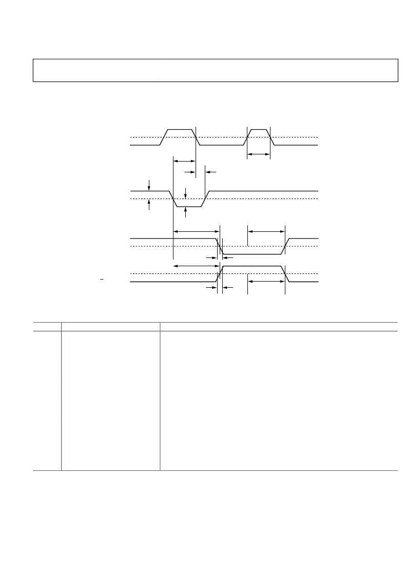
Figure 2 illustrates the ADCMP603 latch timing relationships. Table 2 provides definitions of the terms shown in Figure 2.
Rev. 0 | Page 5 of 16
1.1V
50%
V
N
± V
OS
DIFFERENTIAL
INPUT VOLTAGE
LATCH ENABLE
Q OUTPUT
t
H
t
PDL
t
PLOH
t
F
V
IN
V
OD
t
S
t
PL
0
50%
Q OUTPUT
t
PDH
t
PLOL
t
R
Figure 2. System Timing Diagram
Table 2. Timing Descriptions
Symbol
Timing
t
Input to output high delay
PDH
Description
Propagation delay measured from the time the input signal crosses the reference (± the
input offset voltage) to the 50% point of an output low-to-high transition.
Propagation delay measured from the time the input signal crosses the reference (± the
input offset voltage) to the 50% point of an output high-to-low transition.
Propagation delay measured from the 50% point of the latch enable signal low-to-high
transition to the 50% point of an output low-to-high transition.
Propagation delay measured from the 50% point of the latch enable signal low-to-high
transition to the 50% point of an output high-to-low transition.
Minimum time after the negative transition of the latch enable signal that the input signal
must remain unchanged to be acquired and held at the outputs.
Minimum time that the latch enable signal must be high to acquire an input signal change.
Minimum time before the negative transition of the latch enable signal occurs that an
input signal change must be present to be acquired and held at the outputs.
Amount of time required to transition from a low to a high output as measured at the 20%
and 80% points.
Amount of time required to transition from a high to a low output as measured at the 20%
and 80% points.
Difference between the input voltages V
t
Input to output low delay
PDL
t
Latch enable to output high delay
PLOH
t
Latch enable to output low delay
PLOL
t
Minimum hold time
H
t
t
Minimum latch enable pulse width
Minimum setup time
PL
S
t
Output rise time
R
t
Output fall time
F
V
Voltage overdrive
OD
A
and V .
B
相關(guān)PDF資料 |
PDF描述 |
|---|---|
| ADCMP603BCPZ-R2 | Rail-to-Rail, Very Fast, 2.5 V to 5.5 V, Single-Supply TTL/CMOS Comparator |
| ADCMP603BCPZ-R7 | Rail-to-Rail, Very Fast, 2.5 V to 5.5 V, Single-Supply TTL/CMOS Comparator |
| ADCMP604 | Rail-to-Rail, Very Fast, 2.5 V to 5.5 V, Single-Supply LVDS Comparators |
| ADCMP606 | Rail-to-Rail, Very Fast, 2.5 V to 5.5 V, Single-Supply CML Comparators |
| ADCMP606_0610 | Rail-to-Rail, Very Fast, 2.5 V to 5.5 V, Single-Supply CML Comparators |
相關(guān)代理商/技術(shù)參數(shù) |
參數(shù)描述 |
|---|---|
| ADCMP603BCPZ-R2 | 功能描述:IC COMP TTL/CMOS 1CHAN 12-LFCSP RoHS:是 類(lèi)別:集成電路 (IC) >> 線性 - 比較器 系列:- 產(chǎn)品培訓(xùn)模塊:Lead (SnPb) Finish for COTS Obsolescence Mitigation Program 標(biāo)準(zhǔn)包裝:2,500 系列:- 類(lèi)型:通用 元件數(shù):1 輸出類(lèi)型:CMOS,推挽式,滿擺幅,TTL 電壓 - 電源,單路/雙路(±):2.5 V ~ 5.5 V,±1.25 V ~ 2.75 V 電壓 - 輸入偏移(最小值):5mV @ 5.5V 電流 - 輸入偏壓(最小值):1pA @ 5.5V 電流 - 輸出(標(biāo)準(zhǔn)):- 電流 - 靜態(tài)(最大值):24µA CMRR, PSRR(標(biāo)準(zhǔn)):80dB CMRR,80dB PSRR 傳輸延遲(最大):450ns 磁滯:±3mV 工作溫度:-40°C ~ 85°C 封裝/外殼:6-WFBGA,CSPBGA 安裝類(lèi)型:表面貼裝 包裝:管件 其它名稱(chēng):Q3554586 |
| ADCMP603BCPZ-R7 | 功能描述:IC COMP TTL/CMOS 1CHAN 12-LFCSP RoHS:是 類(lèi)別:集成電路 (IC) >> 線性 - 比較器 系列:- 標(biāo)準(zhǔn)包裝:1 系列:- 類(lèi)型:通用 元件數(shù):1 輸出類(lèi)型:CMOS,開(kāi)路集電極,TTL 電壓 - 電源,單路/雙路(±):2.7 V ~ 5.5 V 電壓 - 輸入偏移(最小值):7mV @ 5V 電流 - 輸入偏壓(最小值):0.25µA @ 5V 電流 - 輸出(標(biāo)準(zhǔn)):84mA @ 5V 電流 - 靜態(tài)(最大值):120µA CMRR, PSRR(標(biāo)準(zhǔn)):- 傳輸延遲(最大):600ns 磁滯:- 工作溫度:-40°C ~ 85°C 封裝/外殼:SC-74A,SOT-753 安裝類(lèi)型:表面貼裝 包裝:剪切帶 (CT) 產(chǎn)品目錄頁(yè)面:1268 (CN2011-ZH PDF) 其它名稱(chēng):*LMV331M5*LMV331M5/NOPBLMV331M5CT |
| ADCMP603BCPZ-WP | 功能描述:IC COMP TTL/CMOS 1CHAN 12-LFCSP RoHS:是 類(lèi)別:集成電路 (IC) >> 線性 - 比較器 系列:- 產(chǎn)品培訓(xùn)模塊:Lead (SnPb) Finish for COTS Obsolescence Mitigation Program 標(biāo)準(zhǔn)包裝:2,500 系列:- 類(lèi)型:通用 元件數(shù):1 輸出類(lèi)型:CMOS,推挽式,滿擺幅,TTL 電壓 - 電源,單路/雙路(±):2.5 V ~ 5.5 V,±1.25 V ~ 2.75 V 電壓 - 輸入偏移(最小值):5mV @ 5.5V 電流 - 輸入偏壓(最小值):1pA @ 5.5V 電流 - 輸出(標(biāo)準(zhǔn)):- 電流 - 靜態(tài)(最大值):24µA CMRR, PSRR(標(biāo)準(zhǔn)):80dB CMRR,80dB PSRR 傳輸延遲(最大):450ns 磁滯:±3mV 工作溫度:-40°C ~ 85°C 封裝/外殼:6-WFBGA,CSPBGA 安裝類(lèi)型:表面貼裝 包裝:管件 其它名稱(chēng):Q3554586 |
| ADCMP604 | 制造商:AD 制造商全稱(chēng):Analog Devices 功能描述:Rail-to-Rail, Very Fast, 2.5 V to 5.5 V, Single-Supply LVDS Comparators |
| ADCMP604_07 | 制造商:AD 制造商全稱(chēng):Analog Devices 功能描述:Rail-to-Rail, Very Fast, 2.5 V to 5.5 V, Single-Supply LVDS Comparators |
發(fā)布緊急采購(gòu),3分鐘左右您將得到回復(fù)。