- 您現在的位置:買賣IC網 > PDF目錄373977 > ADCMP607BCPZ-WP (ANALOG DEVICES INC) Rail-to-Rail, Very Fast, 2.5 V to 5.5 V, Single-Supply CML Comparators PDF資料下載
參數資料
| 型號: | ADCMP607BCPZ-WP |
| 廠商: | ANALOG DEVICES INC |
| 元件分類: | 運動控制電子 |
| 英文描述: | Rail-to-Rail, Very Fast, 2.5 V to 5.5 V, Single-Supply CML Comparators |
| 中文描述: | COMPARATOR, 5000 uV OFFSET-MAX, 2.1 ns RESPONSE TIME, QCC12 |
| 封裝: | 3 X 3 MM, ROHS COMPLIANT, MO-220VEED-1, LFCSP-12 |
| 文件頁數: | 10/16頁 |
| 文件大小: | 280K |
| 代理商: | ADCMP607BCPZ-WP |
ADCMP606/ADCMP607
APPLICATION INFORMATION
POWER/GROUND LAYOUT AND BYPASSING
The ADCMP606/ADCMP607 comparators are very high speed
devices. Despite the low noise output stage, it is essential to use
proper high speed design techniques to achieve the specified
performance. Because comparators are uncompensated
amplifiers, feedback in any phase relationship is likely to cause
oscillations or undesired hysteresis. Of critical importance is the
use of low impedance supply planes, particularly the output
supply plane (V
CCO
) and the ground plane (GND). Individual
supply planes are recommended as part of a multilayer board.
Providing the lowest inductance return path for switching
currents ensures the best possible performance in the target
application.
It is also important to adequately bypass the input and output
supplies. Multiple high quality 0.01 μF bypass capacitors should
be placed as close as possible to each of the V
CCI
and V
CCO
supply
pins and should be connected to the GND plane with redundant
vias. At least one of these should be placed to provide a physically
short return path for output currents flowing back from ground
to the V
CC
pin. High frequency bypass capacitors should be
carefully selected for minimum inductance and ESR. Parasitic
layout inductance should also be strictly controlled to maximize
the effectiveness of the bypass at high frequencies.
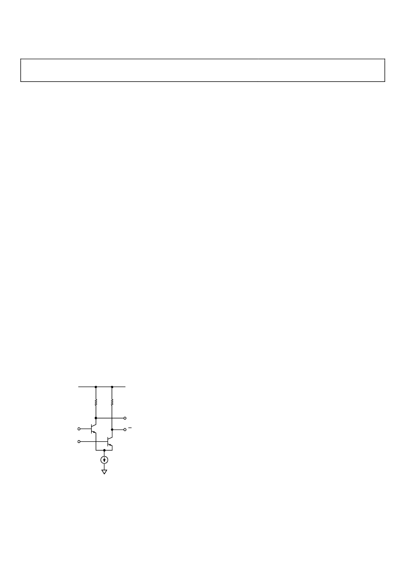
CML-COMPATIBLE OUTPUT STAGE
Specified propagation delay dispersion performance can be
achieved by using proper transmission line terminations. The
outputs of the ADCMP606 and ADCMP607 are designed to drive
400 mV directly into a 50 Ω cable or into transmission lines
terminated using either microstrip or strip line techniques with
50 Ω referenced to V
CC
. The CML output stage is shown in the
simplified schematic diagram in Figure 14. Each output is back-
terminated with 50 Ω for best transmission line matching.
Rev. 0 | Page 10 of 16
Q
16mA
50
Q
V
CCO
GND
0
Figure 14. Simplified Schematic Diagram of
CML-Compatible Output Stage
If these high speed signals must be routed more than a
centimeter, then either microstrip or strip line techniques are
required to ensure proper transition times and to prevent
excessive output ringing and pulse width dependent
propagation delay dispersion.
It is also possible to operate the outputs with the internal
termination only if greater output swing is desired. This can be
especially useful for driving inputs on CMOS devices intended
for full swing ECL and PECL, or for generating pseudo PECL
levels. To avoid deep saturation of the outputs and resulting
pulse dispersion, V
CCO
must be kept above the specified
minimum output low level (see the Electrical Characteristics
section). The line length driven should be kept as short as
possible.
USING/DISABLING THE LATCH FEATURE
The latch input is designed for maximum versatility. It can
safely be left floating or it can be driven low by any standard
TTL/CMOS device as a high speed latch.
In addition, the pin can be operated as a hysteresis control pin
with a bias voltage of 1.25 V nominal and an input resistance of
approximately 7000 Ω. This allows the comparator hysteresis to
be easily controlled by either a resistor or an inexpensive CMOS
DAC. Driving this pin high or floating the pin removes all
hysteresis.
Hysteresis control and latch mode can be used together if an
open drain, an open collector, or a three-state driver is connected
parallel to the hysteresis control resistor or current source.
Due to the programmable hysteresis feature, the logic threshold
of the latch pin is approximately 1.1 V regardless of V
CC
.
OPTIMIZING PERFORMANCE
As with any high speed comparator, proper design and layout
techniques are essential for obtaining the specified performance.
Stray capacitance, inductance, inductive power and ground
impedances, or other layout issues can severely limit performance
and often cause oscillation. Large discontinuities along input
and output transmission lines can also limit the specified pulse
width dispersion performance. The source impedance should
be minimized as much as is practicable. High source impedance,
in combination with the parasitic input capacitance of the
comparator, causes an undesirable degradation in bandwidth at
the input, thus degrading the overall response. Thermal noise
from large resistances can easily cause extra jitter with slowly
slewing input signals; higher impedances encourage undesired
coupling.
相關PDF資料 |
PDF描述 |
|---|---|
| ADCMP609 | Rail-to-Rail, Fast, Low Power 2.5 V to 5.5 V, Single-Supply TTL/CMOS Comparator |
| ADCMP609BRMZ1 | Rail-to-Rail, Fast, Low Power 2.5 V to 5.5 V, Single-Supply TTL/CMOS Comparator |
| ADCMP609BRMZ-REEL1 | Replacement for Texas Instruments part number LM107J. Buy from authorized manufacturer Rochester Electronics. |
| ADCMP609BRMZ-REEL71 | Replacement for Texas Instruments part number LM107JB. Buy from authorized manufacturer Rochester Electronics. |
| ADCMP670 | Dual Low Power 1.5% Comparator With 400 mV Reference |
相關代理商/技術參數 |
參數描述 |
|---|---|
| ADCMP608 | 制造商:AD 制造商全稱:Analog Devices 功能描述:Rail-to-Rail, Fast, Low Power 2.5 V to 5.5 V, Single-Supply TTL/CMOS Comparator |
| ADCMP608_07 | 制造商:AD 制造商全稱:Analog Devices 功能描述:Rail-to-Rail, Fast, Low Power 2.5 V to 5.5 V, Single-Supply TTL/CMOS Comparator |
| ADCMP608BKSZ-R2 | 功能描述:IC COMP TTL/CMOS R-R SGL SC70-6 RoHS:是 類別:集成電路 (IC) >> 線性 - 比較器 系列:- 標準包裝:25 系列:- 類型:帶電壓基準 元件數:4 輸出類型:CMOS,開路漏極,TTL 電壓 - 電源,單路/雙路(±):2 V ~ 11 V,±1 V ~ 5.5 V 電壓 - 輸入偏移(最小值):10mV @ 5V 電流 - 輸入偏壓(最小值):- 電流 - 輸出(標準):0.015mA @ 5V 電流 - 靜態(最大值):8.5µA CMRR, PSRR(標準):80dB CMRR,80dB PSRR 傳輸延遲(最大):12µs 磁滯:50mV 工作溫度:0°C ~ 70°C 封裝/外殼:16-DIP(0.300",7.62mm) 安裝類型:通孔 包裝:管件 |
| ADCMP608BKSZ-REEL | 制造商:AD 制造商全稱:Analog Devices 功能描述:Rail-to-Rail, Fast, Low Power 2.5 V to 5.5 V, Single-Supply TTL/CMOS Comparator |
| ADCMP608BKSZ-REEL7 | 功能描述:IC COMPARATOR TTL/CMOS SC70-6 RoHS:是 類別:集成電路 (IC) >> 線性 - 比較器 系列:- 標準包裝:1 系列:- 類型:通用 元件數:1 輸出類型:CMOS,開路集電極,TTL 電壓 - 電源,單路/雙路(±):2.7 V ~ 5.5 V 電壓 - 輸入偏移(最小值):7mV @ 5V 電流 - 輸入偏壓(最小值):0.25µA @ 5V 電流 - 輸出(標準):84mA @ 5V 電流 - 靜態(最大值):120µA CMRR, PSRR(標準):- 傳輸延遲(最大):600ns 磁滯:- 工作溫度:-40°C ~ 85°C 封裝/外殼:SC-74A,SOT-753 安裝類型:表面貼裝 包裝:剪切帶 (CT) 產品目錄頁面:1268 (CN2011-ZH PDF) 其它名稱:*LMV331M5*LMV331M5/NOPBLMV331M5CT |
發布緊急采購,3分鐘左右您將得到回復。