- 您現在的位置:買賣IC網 > PDF目錄373978 > ADD8708WSTZ-REEL (ANALOG DEVICES INC) 18-Channel Gamma Buffer with Regulator PDF資料下載
參數資料
| 型號: | ADD8708WSTZ-REEL |
| 廠商: | ANALOG DEVICES INC |
| 元件分類: | 運動控制電子 |
| 英文描述: | 18-Channel Gamma Buffer with Regulator |
| 中文描述: | 18 BUFFER AMPLIFIER, PQFP48 |
| 封裝: | LEAD FREE, MO-026-BBC, LQFP-48 |
| 文件頁數: | 1/16頁 |
| 文件大?。?/td> | 454K |
| 代理商: | ADD8708WSTZ-REEL |
18-Channel Gamma Buffer
with Regulator
ADD8708
FEATURES
18 precision gamma reference outputs
Mask-programmable gamma resistors:
0.2% resolution and 0.1% accuracy
Mask-programmable voltage regulator: 0.4% accuracy
Upper 9 buffers swing to V
DD
Lower 9 buffers swing to GND
Single-supply operation: 7.5 V to 16.5 V
Gamma current drive: 15 mA per channel
Peak output current: 150 mA
Output voltage stable under load conditions
Pin-to-pin compatible with ADD8709
48-lead, Pb-free LQFP and LFCSP
APPLICATIONS
LCD TV panels
LCD monitor panels
GENERAL DESCRIPTION
Rev.
0
Information furnished by Analog Devices is believed to be accurate and reliable.
However, no responsibility is assumed by Analog Devices for its use, nor for any
infringements of patents or other rights of third parties that may result from its use.
Specifications subject to change without notice. No license is granted by implication
or otherwise under any patent or patent rights of Analog Devices. Trademarks and
registered trademarks are the property of their respective owners.
One Technology Way, P.O. Box 9106, Norwood, MA 02062-9106, U.S.A.
Tel: 781.329.4700
Fax: 781.326.8703
2004 Analog Devices, Inc. All rights reserved.
www.analog.com
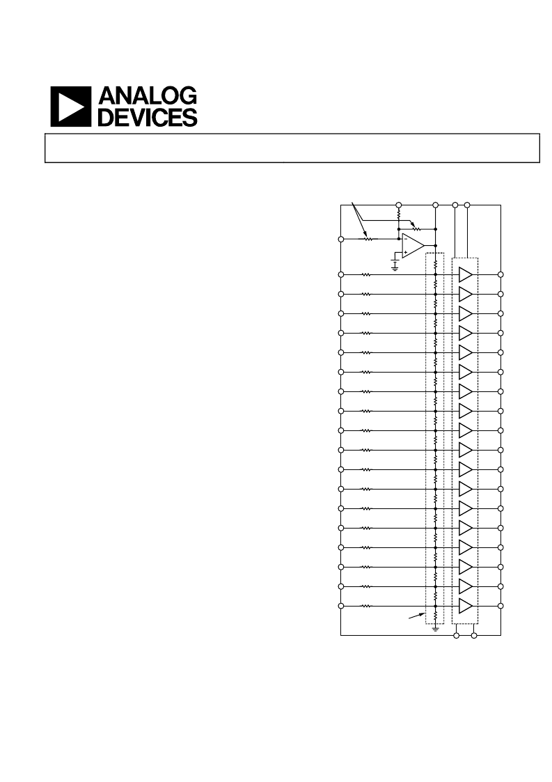
The ADD8708 is an 18-channel integrated gamma reference for
use in high resolution LCD TV and monitors panels. The out-
put buffers feature high current drive and low offset voltage to
provide an accurate and stable gamma curve. The top nine
channels swing to V
DD
; the lower nine channels swing to GND.
Integrating the gamma setup resistors drastically reduces the
external component count while increasing the gamma curve
accuracy. To accommodate multiple column drivers and panel
architectures, the ADD8708 is mask programmable to a 0.2%
resolution using the on-chip 500 resistor string. An on-board
voltage regulator provides a fixed input for the resistor string,
isolating the gamma curve from the supply ripple.
The ADD8708 is specified over the temperature range of
–40
°
C to +105
°
C and comes in both a 48-lead, Pb-free,
lead-frame chip-scale package and a Pb-free, low-profile,
quad flat package.
FUNCTIONAL BLOCK DIAGRAM
0
GND
GND
V
DD
V
DD
V
OUT
18
GAMMA
BUFFERS
V
IN
18
GND
1.2V
+
–
MASK-PROGRAMMABLE
REGULATOR RESISTORS
MASK-PROGRAMMABLE
RESISTOR STRING
V
OUT
17
V
IN
17
V
OUT
16
V
IN
16
V
OUT
15
V
IN
15
V
OUT
14
V
IN
14
V
OUT
13
V
IN
13
V
OUT
12
V
IN
12
V
OUT
11
V
IN
11
V
OUT
10
V
IN
10
V
OUT
9
V
IN
9
V
OUT
8
V
IN
8
V
OUT
7
V
IN
7
V
OUT
6
V
IN
6
V
OUT
5
V
IN
5
V
OUT
4
V
IN
4
V
OUT
3
V
IN
3
V
OUT
2
V
IN
2
V
OUT
1
V
IN
1
FB
V
REG OUT
700
*
700
*
700
*
700
*
700
*
700
*
700
*
700
*
700
*
700
*
700
*
700
*
700
*
700
*
700
*
700
*
700
*
700
*
700
*
*ESD PROTECTION RESISTORS
Figure 1. 48-Lead LQFP or LFCSP
相關PDF資料 |
PDF描述 |
|---|---|
| ADD8709 | 18-Channel Gamma Buffer with Regulator |
| ADD8709ASTZ-REEL | 18-Channel Gamma Buffer with Regulator |
| ADD8709ASTZ-REEL7 | 18-Channel Gamma Buffer with Regulator |
| ADD8710 | 10 - CHANNEL GAMMA BUFFER WITH V-COM DRIVER |
| ADD8710ARUZ | 10 - CHANNEL GAMMA BUFFER WITH V-COM DRIVER |
相關代理商/技術參數 |
參數描述 |
|---|---|
| ADD8709 | 制造商:AD 制造商全稱:Analog Devices 功能描述:18-Channel Gamma Buffer with Regulator |
| ADD8709ASTZ-REEL | 制造商:Rochester Electronics LLC 功能描述: 制造商:Analog Devices 功能描述: |
| ADD8709ASTZ-REEL7 | 制造商:Rochester Electronics LLC 功能描述: 制造商:Analog Devices 功能描述: |
| ADD8709WSTZ-REEL7 | 制造商:Rochester Electronics LLC 功能描述: 制造商:Analog Devices 功能描述: |
| ADD8710 | 制造商:AD 制造商全稱:Analog Devices 功能描述:10 - CHANNEL GAMMA BUFFER WITH V-COM DRIVER |
發布緊急采購,3分鐘左右您將得到回復。