參數資料
| 型號: | ADDAC80-CBI-V |
| 廠商: | Analog Devices Inc |
| 文件頁數: | 1/16頁 |
| 文件大小: | 0K |
| 描述: | IC DAC 12BIT LOW COST 24-CDIP |
| 產品培訓模塊: | Data Converter Fundamentals DAC Architectures |
| 標準包裝: | 1 |
| 設置時間: | 2µs |
| 位數: | 12 |
| 數據接口: | 并聯 |
| 轉換器數目: | 1 |
| 電壓電源: | 雙 ± |
| 功率耗散(最大): | 300mW |
| 工作溫度: | 0°C ~ 70°C |
| 安裝類型: | 通孔 |
| 封裝/外殼: | 24-CDIP(0.600",15.24mm) |
| 供應商設備封裝: | 24-CDIP 側面鍍銅 |
| 包裝: | 管件 |
| 輸出數目和類型: | 1 電壓,單極;1 電壓,雙極 |
| 采樣率(每秒): | * |
REV. B
Information furnished by Analog Devices is believed to be accurate and
reliable. However, no responsibility is assumed by Analog Devices for its
use, nor for any infringements of patents or other rights of third parties that
may result from its use. No license is granted by implication or otherwise
under any patent or patent rights of Analog Devices.
a
ADDAC80/ADDAC85/ADDAC87
One Technology Way, P.O. Box 9106, Norwood, MA 02062-9106, U.S.A.
Tel: 781/329-4700
Fax: 781/326-8703
Analog Devices, Inc., 2002
Complete Low Cost
12-Bit D/A Converters
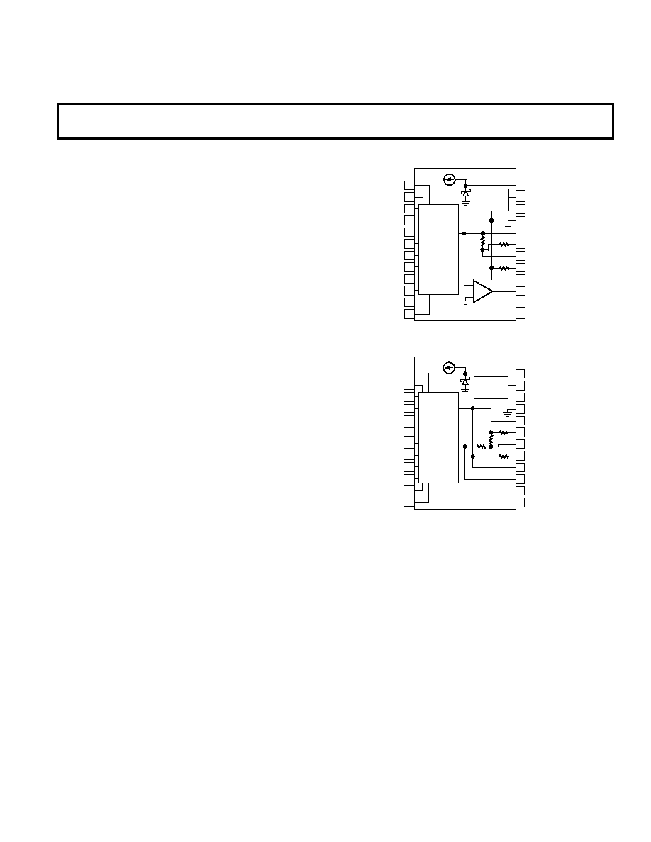
FUNCTIONAL BLOCK DIAGRAM
*NC = CBI VERSIONS
5V – CCD VERSIONS
(MSB) BIT 1
BIT 2
BIT 3
BIT 4
BIT 5
BIT 6
BIT 7
BIT 8
BIT 9
BIT 10
BIT 11
(LSB) BIT 12
VREF OUT
GAIN ADJUST
+VS
COMMON
SUMMING JUNCTION
20V RANGE
10V RANGE
BIPOLAR OFFSET
REF INPUT
VOUT
–VS
NC/+VL*
12-BIT
RESISTOR
LADDER
NETWORK
AND
CURRENT
SWITCHES
REF
CONTROL
CIRCUIT
1
2
3
4
5
6
7
8
9
10
11
12
24
23
22
21
20
19
18
17
16
15
14
13
6.3k
5k
ADDAC80
+
–
*NC = CBI VERSIONS
5V – CCD VERSIONS
(MSB) BIT 1
BIT 2
BIT 3
BIT 4
BIT 5
BIT 6
BIT 7
BIT 8
BIT 9
BIT 10
BIT 11
(LSB) BIT 12
VREF OUT
GAIN ADJUST
+VS
COMMON
SCALING NETWORK
BIPOLAR OFFSET
REF INPUT
IOUT
–VS
NC/+VL*
12-BIT
RESISTOR
LADDER
NETWORK
AND
CURRENT
SWITCHES
REF
CONTROL
CIRCUIT
1
2
3
4
5
6
7
8
9
10
11
12
24
23
22
21
20
19
18
17
16
15
14
13
6.3k
2k
5k
FEATURES
Single Chip Construction
On-Board Output Amplifier
Low Power Dissipation: 300 mW
Monotonicity Guaranteed over Temperature
Guaranteed for Operation with 12 V Supplies
Improved Replacement for Standard DAC80, DAC800
Hl-5680
High Stability, High Current Output
Buried Zener Reference
Laser Trimmed to High Accuracy
1/2 LSB Max Nonlinearity
Low Cost Plastic Packaging
PRODUCT DESCRIPTION
The ADDAC80 Series is a family of low cost 12-bit digital-to-
analog converters with both a high stability voltage reference
and output amplifier combined on a single monolithic chip.
The ADDAC80 Series is recommended for all low cost 12-bit D/A
converter applications where reliability and cost are of paramount
importance.
Advanced circuit design and precision processing techniques
result in significant performance advantages over conventional
DAC80 devices. Innovative circuit design reduces the total
power consumption to 300 mW, which not only improves reli-
ability, but also improves long term stability.
The ADDAC80 incorporates a fully differential, nonsaturating
precision current switching cell structure which provides greatly
increased immunity to supply voltage variation. This same struc-
ture also reduces nonlinearities due to thermal transients as the
various bits are switched; nearly all critical components operate
at constant power dissipation. High stability, SiCr thin film
resistors are trimmed with a fine resolution laser, resulting in
lower differential nonlinearity errors. A low noise, high stability,
subsurface Zener diode is used to produce a reference voltage
with excellent long term stability, high external current capabil-
ity and temperature drift characteristics which challenge the
best discrete Zener references.
The ADDAC80 Series is available in three performance grades
and three package types. The ADDAC80 is specified for use
over the 0
°C to 70°C temperature range and is available in
both plastic and ceramic DIP packages. The ADDAC85 and
ADDAC87 are available in hermetically sealed ceramic packages
and are specified for the –25
°C to +85°C and –55°C to +125°C
temperature ranges.
PRODUCT HIGHLIGHTS
1. The ADDAC80 series of D/A converters directly replaces all
other devices of this type with significant increases in performance.
2. Single chip construction and low power consumption pro-
vides the optimum choice for applications where low cost
and high reliability are major considerations.
3. The high speed output amplifier has been designed to settle
within 1/2 LSB for a 10 V full scale transition in 2.0
s, when
properly compensated.
4. The precision buried Zener reference can supply up to 2.5 mA
for use elsewhere in the application.
5. The low TC binary ladder guarantees that all units are mono-
tonic over the specified temperature range.
6. System performance upgrading is possible without redesign.
相關PDF資料 |
PDF描述 |
|---|---|
| ADG1201BRJZ-R2 | IC SWITCH SPST NO SOT23 |
| ADG1204YRUZ-REEL7 | IC MULTIPLEXER 4X1 14TSSOP |
| ADG1207YRUZ-REEL7 | IC MULTIPLEXER DUAL 8X1 28TSSOP |
| ADG1209YRZ | IC MULTIPLEXER DUAL 4X1 16SOIC |
| ADG1213YCPZ-500RL7 | IC SWITCH QUAD SPST 16LFCSP |
相關代理商/技術參數 |
參數描述 |
|---|---|
| ADDAC80CBI-V | 制造商:AD 功能描述:_ |
| ADDAC80-CCD-I | 制造商:Analog Devices 功能描述:DAC 1-CH Current Steering 12-bit 24-Pin SBCDIP Tube 制造商:Rochester Electronics LLC 功能描述:12-BIT GEN'L PURPOSE D - Bulk |
| ADDAC80-CCD-V | 功能描述:IC DAC 12BIT LOW COST 24-CDIP RoHS:否 類別:集成電路 (IC) >> 數據采集 - 數模轉換器 系列:- 產品培訓模塊:Lead (SnPb) Finish for COTS Obsolescence Mitigation Program 標準包裝:1,000 系列:- 設置時間:1µs 位數:8 數據接口:串行 轉換器數目:8 電壓電源:雙 ± 功率耗散(最大):941mW 工作溫度:0°C ~ 70°C 安裝類型:表面貼裝 封裝/外殼:24-SOIC(0.295",7.50mm 寬) 供應商設備封裝:24-SOIC W 包裝:帶卷 (TR) 輸出數目和類型:8 電壓,單極 采樣率(每秒):* |
| ADDAC80D-CBI-I | 制造商:Analog Devices 功能描述: 制造商:Analog Devices 功能描述:PARALLEL, WORD INPUT LOADING, 1 us SETTLING TIME, 12-BIT DAC, CDIP24 |
| ADDAC80DCBIV | 制造商:AD 制造商全稱:Analog Devices 功能描述:COMPLETE LOW COST 12-BIT D/A CONVERTERS |
發布緊急采購,3分鐘左右您將得到回復。