- 您現在的位置:買賣IC網 > PDF目錄373980 > ADE7751ARSRL (ANALOG DEVICES INC) Energy Metering IC with On-Chip Fault Detection PDF資料下載
參數資料
| 型號: | ADE7751ARSRL |
| 廠商: | ANALOG DEVICES INC |
| 元件分類: | 模擬信號調理 |
| 英文描述: | Energy Metering IC with On-Chip Fault Detection |
| 中文描述: | SPECIALTY ANALOG CIRCUIT, PDSO24 |
| 封裝: | SSOP-24 |
| 文件頁數: | 5/16頁 |
| 文件大小: | 422K |
| 代理商: | ADE7751ARSRL |
REV. 0
ADE7751
–5–
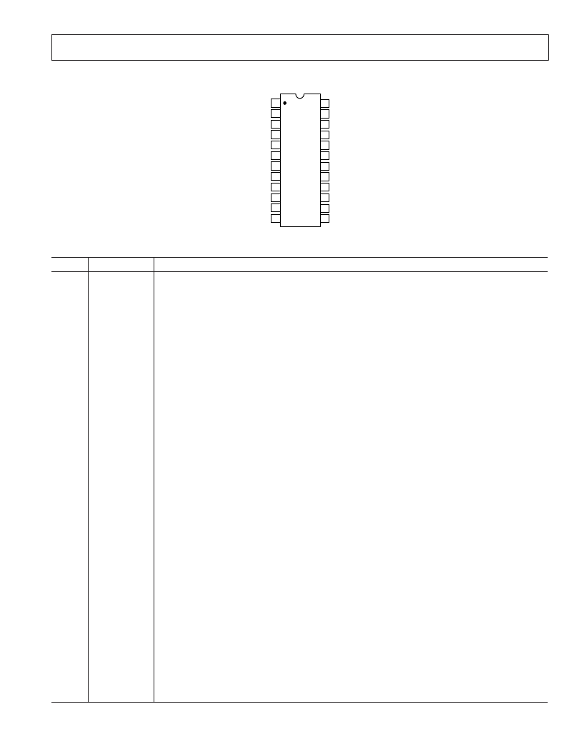
PIN CONFIGURATION
TOP VIEW
(Not to Scale)
24
23
22
21
20
19
18
17
16
15
14
13
1
2
3
4
5
6
7
8
9
10
11
12
ADE7751
SCF
AGND
REF
IN/OUT
RESET
V2P
DV
DD
AC/
DC
AV
DD
V1A
V2N
V1N
V1B
S1
S0
G1
G0
CLKIN
F1
F2
CF
DGND
CLKOUT
FAULT
REVP
PIN FUNCTION DESCRIPTIONS
Pin No.
Mnemonic
Description
1
DV
DD
Digital Power Supply. This pin provides the supply voltage for the digital circuitry in the ADE7751.
The supply voltage should be maintained at 5 V
±
5% for specified operation. This pin should be
decoupled with a 10
μ
F capacitor in parallel with a ceramic 100 nF capacitor.
High-Pass Filter Select. This logic input is used to enable the HPF in Channel 1 (the current
channel). A Logic 1 on this pin enables the HPF. The associated phase response of this filter has
been internally compensated over a frequency range of 45 Hz to 1 kHz. The HPF filter should be
enabled in energy metering applications.
Analog Power Supply. This pin provides the supply voltage for the analog circuitry in the ADE7751.
The supply should be maintained at 5 V
±
5% for specified operation. Every effort should be made
to minimize power supply ripple and noise at this pin by the use of proper decoupling. This pin
should be decoupled to AGND with a 10
μ
F capacitor in parallel with a ceramic 100 nF capacitor.
Analog Inputs for Channel 1 (Current Channel). These inputs are fully differential voltage inputs
with a maximum signal level of
±
660 mV with respect to pin V1N for specified operation. The
maximum signal level at these pins is
±
1 V with respect to AGND. Both inputs have internal ESD
protection circuitry and an overvoltage of
±
6 V can also be sustained on these inputs without risk of
permanent damage.
Negative Input Pin for Differential Voltage Inputs V1A and V1B. The maximum signal level at this
pin is
±
1 V with respect to AGND. The input has internal ESD protection circuitry and an overvoltage
of
±
6 V can also be sustained without risk of permanent damage. This input should be directly con-
nected to the burden resistor and held at a fixed potential, i.e., AGND. See Analog Input section.
Negative and Positive Inputs for Channel 2 (Voltage Channel). These inputs provide a fully differ-
ential input pair. The maximum differential input voltage is
±
660 mV for specified operation. The
maximum signal level at these pins is
±
1 V with respect to AGND. Both inputs have internal ESD
protection circuitry and an overvoltage of
±
6 V can also be sustained on these inputs without risk of
permanent damage.
Reset Pin for the ADE7751. A logic low on this pin will hold the ADCs and digital circuitry in a
reset condition. Bringing this pin logic low will clear the ADE7751 internal registers.
Provides Access to the On-Chip Voltage Reference. The on-chip reference has a nominal value of
2.5 V
±
8% and a typical temperature coefficient of 30 ppm/
°
C. An external reference source may also
be connected at this pin. In either case, this pin should be decoupled to AGND with a 1
μ
F ceramic
capacitor and 100 nF ceramic capacitor.
Provides the Ground Reference for the Analog Circuitry in the ADE7751, i.e., ADCs and Refer-
ence. This pin should be tied to the analog ground plane of the PCB. The analog ground plane is
the ground reference for all analog circuitry, e.g., antialiasing filters, current and voltage trans-
ducers, and more. For good noise suppression, the analog ground plane should only be connected to
the digital ground plane at one point. A star ground configuration will help to keep noisy digital
return currents away from the analog circuits.
Select Calibration Frequency. This logic input is used to select the frequency on the calibration
output CF. Table IV shows how the calibration frequencies are selected.
2
AC/
DC
3
AV
DD
4, 5
V1A, V1B
6
V1N
7, 8
V2N, V2P
9
RESET
10
REF
IN/OUT
11
AGND
12
SCF
相關PDF資料 |
PDF描述 |
|---|---|
| ADE7752B | Polyphase Energy Metering IC with Pulsed Output |
| ADE7752BARW | Polyphase Energy Metering IC with Pulsed Output |
| ADE7752BARW-RL | Polyphase Energy Metering IC with Pulsed Output |
| ADE7752BARWZ | Polyphase Energy Metering IC with Pulsed Output |
| ADE7752BARWZ-RL | Polyphase Energy Metering IC with Pulsed Output |
相關代理商/技術參數 |
參數描述 |
|---|---|
| ADE7751ARSZ | 功能描述:IC ENERGY METERING 1PHASE 24SSOP RoHS:是 類別:集成電路 (IC) >> PMIC - 能量測量 系列:- 產品培訓模塊:Lead (SnPb) Finish for COTS Obsolescence Mitigation Program 標準包裝:2,500 系列:* |
| ADE7751ARSZRL | 功能描述:IC ENERGY METERING 1PHASE 24SSOP RoHS:是 類別:集成電路 (IC) >> PMIC - 能量測量 系列:- 產品培訓模塊:Lead (SnPb) Finish for COTS Obsolescence Mitigation Program 標準包裝:2,500 系列:* |
| ADE7752 | 制造商:AD 制造商全稱:Analog Devices 功能描述:Three Phase Energy Metering IC with Pulse Output |
| ADE7752A | 制造商:AD 制造商全稱:Analog Devices 功能描述:Polyphase Energy Metering IC with Pulse Output |
| ADE7752AAR | 制造商:Analog Devices 功能描述:IC ENERGY METER |
發布緊急采購,3分鐘左右您將得到回復。