- 您現在的位置:買賣IC網 > PDF目錄373980 > ADE7752B (Analog Devices, Inc.) Polyphase Energy Metering IC with Pulsed Output PDF資料下載
參數資料
| 型號: | ADE7752B |
| 廠商: | Analog Devices, Inc. |
| 英文描述: | Polyphase Energy Metering IC with Pulsed Output |
| 中文描述: | 多相電能計量IC脈沖輸出 |
| 文件頁數: | 7/27頁 |
| 文件大小: | 342K |
| 代理商: | ADE7752B |
第1頁第2頁第3頁第4頁第5頁第6頁當前第7頁第8頁第9頁第10頁第11頁第12頁第13頁第14頁第15頁第16頁第17頁第18頁第19頁第20頁第21頁第22頁第23頁第24頁第25頁第26頁第27頁
Preliminary Technical Data
ADE7752B
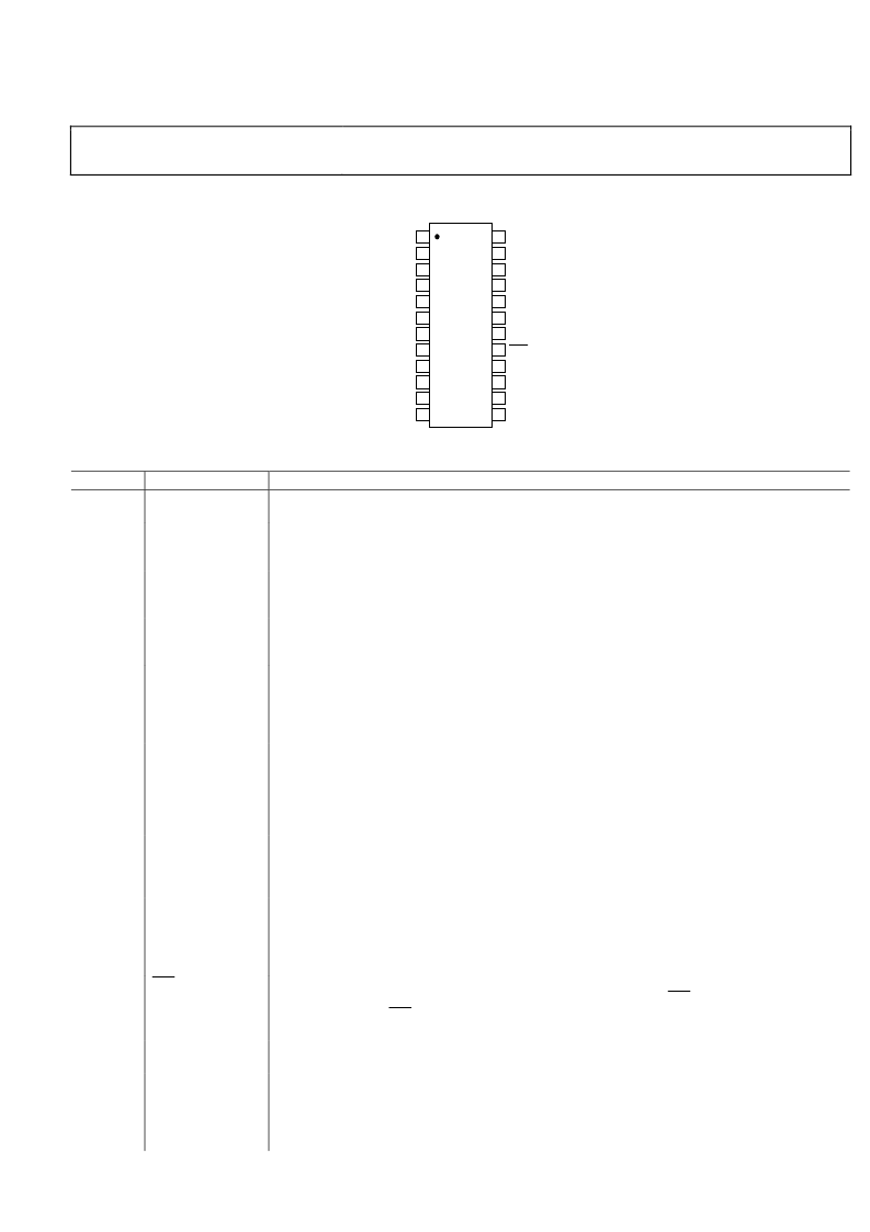
PIN CONFIGURATION AND FUNCTION DESCRIPTIONS
Rev. PrA | Page 7 of 27
TOP VIEW
(Not to Scale)
ADE7752B
REF
IN/OUT
AGND
ICN
ICP
IBN
CF
DGND
V
DD
REVP
IBP
IAN
IAP
VN
VCP
VBP
VAP
ABS
S0
F2
S1
F1
SCF
CLKIN
CLKOUT
2
3
4
5
6
7
8
9
10
11
12
1
24
23
22
21
20
19
18
17
16
15
14
13
0
Figure 3. Pin Configuration
Table 4. Pin Function Descriptions
Pin No.
Mnemonic
1
CF
Description
Calibration Frequency Logic Output. The CF logic output gives instantaneous active power information.
This output is intended to be used for calibration purposes.
This provides the ground reference for the digital circuitry in the ADE7752B, that is, multiplier, filters,
and digital-to-frequency converter. Because the digital return currents in the ADE7752B are small, it is
acceptable to connect this pin to the analog ground plane of the whole system.
Power Supply. This pin provides the supply voltage for the digital circuitry in the ADE7752B. The supply
voltage should be maintained at 5 V ± 5% for specified operation. This pin should be decoupled to
DGND with a 10 μF capacitor in parallel with a 100 nF ceramic capacitor.
This logic output goes logic high when negative power is detected on the sum of the three phase
powers. This output is not latched and resets when positive power is once again detected (see the
Negative Power Information section).
Analog Inputs for Current Channels. These channels are intended for use with current transducers and
are referenced in this document as current channels. These inputs are fully differential voltage inputs
with maximum differential input signal levels of ±0.5 V (see the Analog Inputs section). Both inputs
have internal ESD protection circuitry; in addition, an overvoltage of ±6 V can be sustained on these
inputs without risk of permanent damage.
This pin provides the ground reference for the analog circuitry in the ADE7752B (ADCs and reference).
This pin should be tied to the analog ground plane or the quietest ground reference in the system. This
quiet ground reference should be used for all analog circuitry, such as, anti-aliasing filters and current
and voltage transducers. To keep ground noise around the ADE7752B to a minimum, the quiet ground
plane should only connect to the digital ground plane at one point. It is acceptable to place the entire
device on the analog ground plane.
This pin provides access to the on-chip voltage reference. The on-chip reference has a nominal value of
2.4 V ±8% and a typical temperature coefficient of 25 ppm/°C. An external reference source can also be
connected at this pin. In either case, this pin should be decoupled to AGND with a 1 μF ceramic
capacitor.
Analog Inputs for the Voltage Channels. These channels are intended for use with voltage transducers
and are referenced in this document as voltage channels. These inputs are single-ended voltage inputs
with a maximum signal level of ±0.5 V with respect to VN for specified operation. All inputs have
internal ESD protection circuitry; in addition, an overvoltage of ±6 V can be sustained on these inputs
without risk of permanent damage.
This logic input is used to select the method by which the three active energies from each phase are
summed. It selects between the arithmetical sum of the three energies (ABS logic high) or the sum of
the absolute values (ABS logic low). See the Mode Selection of the Sum of the Three Active Energies
section.
Select Calibration Frequency. This logic input is used to select the frequency on the calibration output
CF. Table 7 shows how the calibration frequencies are selected.
Master Clock for the ADCs and Digital Signal Processing. An external clock can be provided at this logic
input. Alternatively, a parallel resonant AT crystal can be connected across CLKIN and CLKOUT to
provide a clock source for the ADE7752B. The clock frequency for the specified operation is 10 MHz.
Ceramic load capacitors between 22 pF and 33 pF should be used with the gate oscillator circuit. Refer
to the crystal manufacturer’s data sheet for the load capacitance requirements.
2
DGND
3
V
DD
4
REVP
5, 6;
7, 8;
9, 10
IAP, IAN;
IBP, IBN;
ICP, ICN
11
AGND
12
REF
IN/OUT
13, 14, 15,
16
VN, VCP, VBP, VAP
17
ABS
18
SCF
19
CLKIN
相關PDF資料 |
PDF描述 |
|---|---|
| ADE7752BARW | Polyphase Energy Metering IC with Pulsed Output |
| ADE7752BARW-RL | Polyphase Energy Metering IC with Pulsed Output |
| ADE7752BARWZ | Polyphase Energy Metering IC with Pulsed Output |
| ADE7752BARWZ-RL | Polyphase Energy Metering IC with Pulsed Output |
| ADE7753 | Active and Apparent Energy Metering IC with di/dt sensor interface |
相關代理商/技術參數 |
參數描述 |
|---|---|
| ADE7752BARW | 制造商:AD 制造商全稱:Analog Devices 功能描述:Polyphase Energy Metering IC with Pulsed Output |
| ADE7752BARW-RL | 制造商:AD 制造商全稱:Analog Devices 功能描述:Polyphase Energy Metering IC with Pulsed Output |
| ADE7752BARWZ | 功能描述:IC ENERGY METERING 3PHASE 24SOIC RoHS:是 類別:集成電路 (IC) >> PMIC - 能量測量 系列:- 產品培訓模塊:Lead (SnPb) Finish for COTS Obsolescence Mitigation Program 標準包裝:2,500 系列:* |
| ADE7752BARWZ-RL | 功能描述:IC ENERGY METERING 3PHASE 24SOIC RoHS:是 類別:集成電路 (IC) >> PMIC - 能量測量 系列:- 產品培訓模塊:Lead (SnPb) Finish for COTS Obsolescence Mitigation Program 標準包裝:2,500 系列:* |
| ADE7753 | 制造商:AD 制造商全稱:Analog Devices 功能描述:Active and Apparent Energy Metering IC with di/dt sensor interface |
發布緊急采購,3分鐘左右您將得到回復。