- 您現(xiàn)在的位置:買賣IC網(wǎng) > PDF目錄373981 > ADF4108BCPZ-RL (ANALOG DEVICES INC) PLL Frequency Synthesizer PDF資料下載
參數(shù)資料
| 型號(hào): | ADF4108BCPZ-RL |
| 廠商: | ANALOG DEVICES INC |
| 元件分類: | XO, clock |
| 英文描述: | PLL Frequency Synthesizer |
| 中文描述: | PLL FREQUENCY SYNTHESIZER, 8000 MHz, QCC20 |
| 封裝: | 4 X 4 MM, LEAD FREE, LFCSP-20 |
| 文件頁數(shù): | 10/20頁 |
| 文件大小: | 350K |
| 代理商: | ADF4108BCPZ-RL |
ADF4108
Rev. 0 | Page 10 of 20
HI
HI
D1
D2
Q1
Q2
CLR2
CP
U1
U2
UP
DOWN
ABP2
ABP1
CPGND
U3
R DIVIDER
PROGRAMMABLE
DELAY
N DIVIDER
V
P
CHARGE
PUMP
CLR1
0
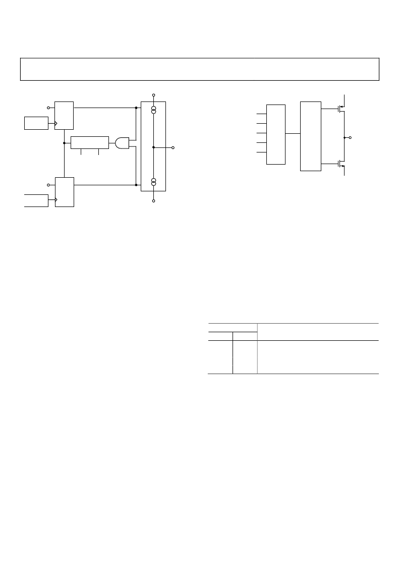
Figure 14. PFD Simplified Schematic and Timing (in Lock)
MUXOUT AND LOCK DETECT
The output multiplexer on the ADF4108 allows the user to
access various internal points on the chip. The state of
MUXOUT is controlled by M3, M2, and M1 in the function
latch. Figure 19 shows the full truth table. Figure 15 shows the
MUXOUT section in block diagram form.
Lock Detect
MUXOUT can be programmed for two types of lock detect:
digital lock detect and analog lock detect.
Digital lock detect is active high. When the lock detect
precision (LDP) bit in the R counter latch is set to 0, digital lock
detect is set high when the phase error on three consecutive
phase detector (PD) cycles is less than 15 ns. With LDP set to 1,
five consecutive cycles of less than 15 ns are required to set the
lock detect. It will stay set high until a phase error of greater
than 25 ns is detected on any subsequent PD cycle.
The N-channel open-drain analog lock detect should be
operated with an external pull-up resistor of 10 kΩ nominal.
When lock has been detected, this output will be high with
narrow, low-going pulses.
DGND
DV
DD
CONTROL
MUX
ANALOG LOCK DETECT
DIGITAL LOCK DETECT
R COUNTER OUTPUT
N COUNTER OUTPUT
SDOUT
MUXOUT
0
Figure 15. MUXOUT Circuit
INPUT SHIFT REGISTER
The ADF4108 digital section includes a 24-bit input shift
register, a 14-bit R counter, and a 19-bit N counter, comprising a
6-bit A counter and a 13-bit B counter. Data is clocked into the
24-bit shift register on each rising edge of CLK. The data is
clocked in MSB first. Data is transferred from the shift register
to one of four latches on the rising edge of LE. The destination
latch is determined by the state of the two control bits (C2, C1)
in the shift register. These are the 2 LSBs, DB1 and DB0, as
shown in the timing diagram of Figure 2. The truth table for
these bits is shown in Table 5.
Figure 16 shows a summary of how the latches are
programmed.
Table 5. C2 and C1 Truth Table
Control Bits
C2
C1
Data Latch
0
0
R counter
0
1
N counter (A and B)
1
0
Function latch (Including prescaler)
1
1
Initialization latch
相關(guān)PDF資料 |
PDF描述 |
|---|---|
| ADF4108BCPZ-RL7 | PLL Frequency Synthesizer |
| ADF4108BRUZ | PLL Frequency Synthesizer |
| ADF4108BRUZ-RL | PLL Frequency Synthesizer |
| ADF4108BRUZ-RL7 | PLL Frequency Synthesizer |
| ADF4113BCHIPS | Circular Connector; No. of Contacts:37; Series:LJT06R; Body Material:Aluminum; Connecting Termination:Crimp; Connector Shell Size:15; Circular Contact Gender:Socket; Circular Shell Style:Straight Plug; Insert Arrangement:15-35 |
相關(guān)代理商/技術(shù)參數(shù) |
參數(shù)描述 |
|---|---|
| ADF4108BCPZ-RL7 | 功能描述:IC PLL FREQUENCY SYNTH 20-LFCSP RoHS:是 類別:集成電路 (IC) >> 時(shí)鐘/計(jì)時(shí) - 時(shí)鐘發(fā)生器,PLL,頻率合成器 系列:- 標(biāo)準(zhǔn)包裝:1,000 系列:Precision Edge® 類型:時(shí)鐘/頻率合成器 PLL:無 輸入:CML,PECL 輸出:CML 電路數(shù):1 比率 - 輸入:輸出:2:1 差分 - 輸入:輸出:是/是 頻率 - 最大:10.7GHz 除法器/乘法器:無/無 電源電壓:2.375 V ~ 3.6 V 工作溫度:-40°C ~ 85°C 安裝類型:表面貼裝 封裝/外殼:16-VFQFN 裸露焊盤,16-MLF? 供應(yīng)商設(shè)備封裝:16-MLF?(3x3) 包裝:帶卷 (TR) 其它名稱:SY58052UMGTRSY58052UMGTR-ND |
| ADF4108BRUZ | 制造商:Analog Devices 功能描述:PLL FREQ SYNTHESIZER SGL UP TO 325MHZ 16TSSOP - Rail/Tube |
| ADF4108BRUZ-RL | 制造商:AD 制造商全稱:Analog Devices 功能描述:PLL Frequency Synthesizer |
| ADF4108BRUZ-RL7 | 制造商:AD 制造商全稱:Analog Devices 功能描述:PLL Frequency Synthesizer |
| ADF4108L703F | 制造商:AD 制造商全稱:Analog Devices 功能描述:PLL Frequency Synthesizer |
發(fā)布緊急采購,3分鐘左右您將得到回復(fù)。