- 您現在的位置:買賣IC網 > PDF目錄373982 > ADF4113HVBCPZ-RL7 (ANALOG DEVICES INC) High Voltage Charge Pump, PLL Synthesizer PDF資料下載
參數資料
| 型號: | ADF4113HVBCPZ-RL7 |
| 廠商: | ANALOG DEVICES INC |
| 元件分類: | XO, clock |
| 英文描述: | High Voltage Charge Pump, PLL Synthesizer |
| 中文描述: | PLL FREQUENCY SYNTHESIZER, 3700 MHz, QCC20 |
| 封裝: | 4 X 4 MM, LEAD FREE, MO-220VGGD-1, LFCSP-20 |
| 文件頁數: | 6/20頁 |
| 文件大小: | 385K |
| 代理商: | ADF4113HVBCPZ-RL7 |
ADF4113HV
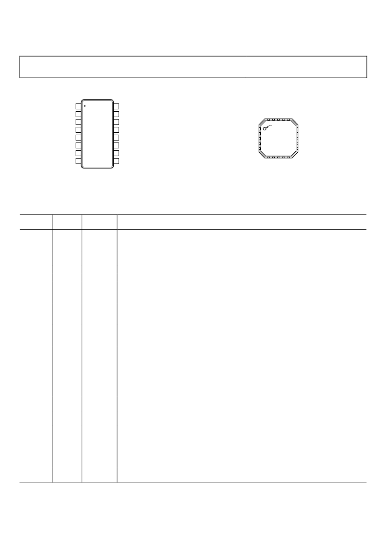
PIN CONFIGURATIONS AND FUNCTION DESCRIPTIONS
Rev. 0 | Page 6 of 20
1
2
3
4
5
6
7
8
CP
CPGND
AGND
AV
DD
R
FIN
A
R
FIN
B
R
SET
REF
IN
16
15
14
13
12
11
10
9
DV
DD
MUXOUT
LE
CE
DGND
CLK
DATA
V
P
ADF4113HV
TOP VIEW
(Not to Scale)
0
Figure 3. TSSOP Pin Configuration
PIN 1
1
2
3
4
5
CPGND
AGND
AGND
RF
IN
B
RF
IN
A
13 DATA
12 CLK
11 CE
14 LE
15 MUXOUT
6
A
D
7
A
D
8
R
I
1
D
9
D
1
P
1
S
2
1
D
1
D
ADF4113HV
TOP VIEW
(Not to Scale)
0
Figure 4. LFCSP Pin Configuration
Table 5. Pin Function Descriptions
TSSOP
Pin No.
Pin No.
1
19
LFCSP
Mnemonic
R
SET
Description
Connecting a resistor between this pin and CPGND sets the maximum charge pump output current.
The nominal voltage potential at the R
SET
pin is 0.56 V for the ADF4113HV. The relationship between
I
CP
and R
SET
is I
CPmax
= 3/R
SET
. Therefore, with R
SET
= 4.7 kΩ, I
CPmax
= 640 μA.
Charge Pump Output. When enabled, this pin provides ±I
CP
to the external loop filter; in turn, this
drives the external VCO.
Charge Pump Ground. CPGND is the ground return path for the charge pump.
Analog Ground. This is the ground return path of the prescaler.
Complementary Input to the RF Prescaler. This point should be decoupled to the ground plane with
a small bypass capacitor, typically 100 pF.
Input to the RF Prescaler. This small-signal input is ac-coupled from the VCO.
Analog Power Supply. The power supply can range from 2.7 V to 5.5 V. Decoupling capacitors to the
analog ground plane should be placed as close as possible to this pin. AV
DD
must be the same value
as DV
DD
.
Reference Input. This pin is a CMOS input with a nominal threshold of V
DD
/2, and an equivalent
input resistance of 100 kΩ. This input can be driven from a TTL or CMOS crystal oscillator, or can be
ac-coupled.
Digital Ground.
Chip Enable. A Logic low on this pin powers down the device and puts the charge pump output
into three-state mode. Taking the pin high powers up the device depending on the status of the
Power-Down Bit PD1.
Serial Clock Input. This serial clock is used to clock in the serial data to the registers. The data is
latched into the 24-bit shift register on the CLK rising edge. This input is a high impedance CMOS
input.
Serial Data Input. The serial data is loaded MSB first with the two LSBs being the control bits. This
input is a high impedance CMOS input.
Load Enable, CMOS Input. When LE goes high, the data stored in the shift registers is loaded into
one of the four latches; the latch is selected using the control bits.
Multiplexer Output. This multiplexer output allows either the lock detect, the scaled RF, or the
scaled reference frequency to be externally accessed.
Digital Power Supply. This can range from 2.7 V to 5.5 V. Decoupling capacitors to the digital ground
plane (1μF, 1nF) should be placed as close as possible to this pin. For best performance, the 1 μF
capacitor should be placed within 2 mm of the pin. The placing of the 1nF capacitor is less critical
but should still be within 5 mm of the pin. DV
DD
must have the same value as AV
DD
.
Charge Pump Power Supply. V
P
can range from 13.5 V to 16.5 V and should be decoupled
appropriately.
2
20
CP
3
4
5
1
2, 3
4
CPGND
AGND
RF
IN
B
6
7
5
6, 7
RF
IN
A
AV
DD
8
8
REF
IN
9
10
9, 10
11
DGND
CE
11
12
CLK
12
13
DATA
13
14
LE
14
15
MUXOUT
15
16, 17
DV
DD
16
18
V
P
相關PDF資料 |
PDF描述 |
|---|---|
| ADF4113HVBRUZ | High Voltage Charge Pump, PLL Synthesizer |
| ADF4113HVBRUZ-RL | High Voltage Charge Pump, PLL Synthesizer |
| ADF4113HVBRUZ-RL7 | High Voltage Charge Pump, PLL Synthesizer |
| ADF4116 | PLL Frequency Synthesizer(PLL頻率合成器) |
| ADF4118 | RF PLL Frequency Synthesizers |
相關代理商/技術參數 |
參數描述 |
|---|---|
| ADF4113HVBRUZ | 功能描述:IC CHARGE PUMP HV SYNTH 16-TSSOP RoHS:是 類別:集成電路 (IC) >> 時鐘/計時 - 時鐘發生器,PLL,頻率合成器 系列:- 標準包裝:2,000 系列:- 類型:PLL 頻率合成器 PLL:是 輸入:晶體 輸出:時鐘 電路數:1 比率 - 輸入:輸出:1:1 差分 - 輸入:輸出:無/無 頻率 - 最大:1GHz 除法器/乘法器:是/無 電源電壓:4.5 V ~ 5.5 V 工作溫度:-20°C ~ 85°C 安裝類型:表面貼裝 封裝/外殼:16-LSSOP(0.175",4.40mm 寬) 供應商設備封裝:16-SSOP 包裝:帶卷 (TR) 其它名稱:NJW1504V-TE1-NDNJW1504V-TE1TR |
| ADF4113HVBRUZ-RL | 功能描述:IC CHARGE PUMP HV SYNTH 16-TSSOP RoHS:是 類別:集成電路 (IC) >> 時鐘/計時 - 時鐘發生器,PLL,頻率合成器 系列:- 標準包裝:1,000 系列:Precision Edge® 類型:時鐘/頻率合成器 PLL:無 輸入:CML,PECL 輸出:CML 電路數:1 比率 - 輸入:輸出:2:1 差分 - 輸入:輸出:是/是 頻率 - 最大:10.7GHz 除法器/乘法器:無/無 電源電壓:2.375 V ~ 3.6 V 工作溫度:-40°C ~ 85°C 安裝類型:表面貼裝 封裝/外殼:16-VFQFN 裸露焊盤,16-MLF? 供應商設備封裝:16-MLF?(3x3) 包裝:帶卷 (TR) 其它名稱:SY58052UMGTRSY58052UMGTR-ND |
| ADF4113HVBRUZ-RL7 | 功能描述:IC CHARGE PUMP HV SYNTH 16-TSSOP RoHS:是 類別:集成電路 (IC) >> 時鐘/計時 - 時鐘發生器,PLL,頻率合成器 系列:- 標準包裝:1,000 系列:Precision Edge® 類型:時鐘/頻率合成器 PLL:無 輸入:CML,PECL 輸出:CML 電路數:1 比率 - 輸入:輸出:2:1 差分 - 輸入:輸出:是/是 頻率 - 最大:10.7GHz 除法器/乘法器:無/無 電源電壓:2.375 V ~ 3.6 V 工作溫度:-40°C ~ 85°C 安裝類型:表面貼裝 封裝/外殼:16-VFQFN 裸露焊盤,16-MLF? 供應商設備封裝:16-MLF?(3x3) 包裝:帶卷 (TR) 其它名稱:SY58052UMGTRSY58052UMGTR-ND |
| ADF4113HVSD1Z | 制造商:Analog Devices 功能描述:- Rail/Tube |
| ADF4116 | 制造商:AD 制造商全稱:Analog Devices 功能描述:RF PLL Frequency Synthesizers |
發布緊急采購,3分鐘左右您將得到回復。