- 您現在的位置:買賣IC網 > PDF目錄373982 > ADF4118 (Analog Devices, Inc.) RF PLL Frequency Synthesizers PDF資料下載
參數資料
| 型號: | ADF4118 |
| 廠商: | Analog Devices, Inc. |
| 英文描述: | RF PLL Frequency Synthesizers |
| 中文描述: | 射頻鎖相環頻率合成器 |
| 文件頁數: | 20/20頁 |
| 文件大小: | 226K |
| 代理商: | ADF4118 |
ADF4116/ADF4117/ADF4118
–
20
–
REV. 0
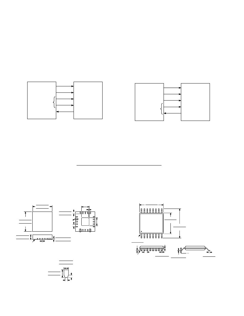
ADuC812 Interface
Figure 29 shows the interface between the ADF4116 family and
the ADuC812 microconverter. Since the ADuC812 is based on
an 8051 core, this interface can be used with any 8051-based
microcontroller. The microconverter is set up for SPI Master
Mode with CPHA = 0. To initiate the operation, the I/O port
driving LE is brought low. Each latch of the ADF4116 family
needs a 24-bit word. This is accomplished by writing three 8-bit
bytes from the microconverter to the device. When the third
byte has been written the LE input should be brought high to
complete the transfer.
SCLOCK
MOSI
I/O PORTS
ADuC812
SCLK
SDATA
LE
CE
MUXOUT
(LOCK DETECT)
ADF4116/
ADF4117/
ADF4118
Figure 29. ADuC812 to ADF4116 Family Interface
On first applying power to the ADF4116 family, it needs three
writes (one each to the R counter latch, the N counter latch and
the initialization latch) for the output to become active.
I/O port lines on the ADuC812 are also used to control power-
down (CE input) and to detect lock (MUXOUT configured as
lock detect and polled by the port input).
When operating in the mode described, the maximum SCLOCK
rate of the ADuC812 is 4 MHz. This means that the maximum
rate at which the output frequency can be changed will be 166 kHz.
ADSP-2181 Interface
Figure 30 shows the interface between the ADF4116 family and
the ADSP-21xx Digital Signal Processor. The ADF4116 family
needs a 21-bit serial word for each latch write. The easiest way
to accomplish this using the ADSP-21xx family is to use the
Autobuffered Transmit Mode of operation with Alternate Fram-
ing. This provides a means for transmitting an entire block of
serial data before an interrupt is generated.
SCLK
DT
I/O FLAGS
ADSP-21xx
SCLK
SDATA
LE
CE
MUXOUT
(LOCK DETECT)
ADF4116/
ADF4117/
ADF4118
TFS
Figure 30. ADSP-21xx to ADF4116 Family Interface
Set up the word length for 8 bits and use three memory loca-
tions for each 24-bit word. To program each 21-bit latch, store
the three 8-bit bytes, enable the Autobuffered mode and then
write to the transmit register of the DSP. This last operation
initiates the autobuffer transfer.
OUTLINE DIMENSIONS
Dimensions shown in inches and (mm).
Chip Scale
(CP-20)
1
20
5
6
10
16
11
15
BOTTOM VIEW
(ROTATED 180 )
0.014 (0.35) 45
°
0.018 (0.45)
0.016 (0.40)
0.014 (0.35)
0.079 (2.0) REF
0.079
(2.0)
REF
DETAIL E
0.020 (0.5) REF
LEAD PITCH
0.0079 (0.20)
REF
0.0083 (0.211)
0.0079 (0.200)
0.0077 (0.195)
SEATING
PLANE
0.039 (1.00)
0.035 (0.90)
0.031 (0.80)
0.159 (4.05)
0.157 (4.00)
0.156 (3.95)
TOP VIEW
0.159 (4.05)
0.157 (4.00)
0.156 (3.95)
0.0059 (0.15)
REF
0.011 (0.275)
0.010 (0.250)
0.009 (0.225)
0.0059
(0.15)
REF
0.018 (0.45)
0.016 (0.40)
0.014 (0.35)
LEAD OPTION
DETAIL E
CONTROLLING DIMENSIONS ARE IN MILLIMETERS
Thin Shrink Small Outline
(RU-16)
16
9
8
1
0.256 (6.50)
0.246 (6.25)
0.177 (4.50)
0.169 (4.30)
PIN 1
0.006 (0.15)
0.002 (0.05)
0.201 (5.10)
0.193 (4.90)
SEATING
PLANE
0.0118 (0.30)
0.0075 (0.19)
0.0256 (0.65)
BSC
0.0433 (1.10)
MAX
0.0079 (0.20)
0.0035 (0.090)
0.028 (0.70)
0.020 (0.50)
8
0
C
–
5
–
4
P
相關PDF資料 |
PDF描述 |
|---|---|
| ADF4117BCP | BATT LITHIUM COIN 3V 48MAH COIN-W/LEGS 12.5MM |
| ADF4117BRU | RF PLL Frequency Synthesizers |
| ADF4118BCP | RF PLL Frequency Synthesizers |
| ADF4118BRU | RF PLL Frequency Synthesizers |
| ADF4116BCP | RF PLL Frequency Synthesizers |
相關代理商/技術參數 |
參數描述 |
|---|---|
| ADF4118BCP | 制造商:AD 制造商全稱:Analog Devices 功能描述:RF PLL Frequency Synthesizers |
| ADF4118BRU | 功能描述:IC SYNTH PLL RF 3.0GHZ 16-TSSOP RoHS:否 類別:集成電路 (IC) >> 時鐘/計時 - 時鐘發生器,PLL,頻率合成器 系列:- 標準包裝:1,000 系列:Precision Edge® 類型:時鐘/頻率合成器 PLL:無 輸入:CML,PECL 輸出:CML 電路數:1 比率 - 輸入:輸出:2:1 差分 - 輸入:輸出:是/是 頻率 - 最大:10.7GHz 除法器/乘法器:無/無 電源電壓:2.375 V ~ 3.6 V 工作溫度:-40°C ~ 85°C 安裝類型:表面貼裝 封裝/外殼:16-VFQFN 裸露焊盤,16-MLF? 供應商設備封裝:16-MLF?(3x3) 包裝:帶卷 (TR) 其它名稱:SY58052UMGTRSY58052UMGTR-ND |
| ADF4118BRU-REEL | 制造商:Analog Devices 功能描述:PLL Frequency Synthesizer Single 16-Pin TSSOP T/R 制造商:Rochester Electronics LLC 功能描述:SINGLE PLL, 3.0GHZ - Tape and Reel |
| ADF4118BRU-REEL7 | 功能描述:IC PLL FREQ SYNTHESIZER 16-TSSOP RoHS:否 類別:集成電路 (IC) >> 時鐘/計時 - 時鐘發生器,PLL,頻率合成器 系列:- 標準包裝:1,000 系列:Precision Edge® 類型:時鐘/頻率合成器 PLL:無 輸入:CML,PECL 輸出:CML 電路數:1 比率 - 輸入:輸出:2:1 差分 - 輸入:輸出:是/是 頻率 - 最大:10.7GHz 除法器/乘法器:無/無 電源電壓:2.375 V ~ 3.6 V 工作溫度:-40°C ~ 85°C 安裝類型:表面貼裝 封裝/外殼:16-VFQFN 裸露焊盤,16-MLF? 供應商設備封裝:16-MLF?(3x3) 包裝:帶卷 (TR) 其它名稱:SY58052UMGTRSY58052UMGTR-ND |
| ADF4118BRU-RL | 制造商:Analog Devices 功能描述:Single PLL, 3.0GHz |
發布緊急采購,3分鐘左右您將得到回復。