- 您現(xiàn)在的位置:買賣IC網(wǎng) > PDF目錄373982 > ADF4210BRU (ANALOG DEVICES INC) Dual RF/IF PLL Frequency Synthesizers PDF資料下載
參數(shù)資料
| 型號: | ADF4210BRU |
| 廠商: | ANALOG DEVICES INC |
| 元件分類: | XO, clock |
| 英文描述: | Dual RF/IF PLL Frequency Synthesizers |
| 中文描述: | PLL FREQUENCY SYNTHESIZER, 1200 MHz, PDSO20 |
| 封裝: | TSSOP-20 |
| 文件頁數(shù): | 19/20頁 |
| 文件大小: | 251K |
| 代理商: | ADF4210BRU |
REV. A
ADF4210/ADF4211/ADF4212/ADF4213
–19–
PCB Guidelines for Chip Scale Package
The lands on the chip scale package (CP-20), are rectangular.
The printed circuit board pad for these should be 0.1 mm
longer than the package land length and 0.05 mm wider than
the package land width. The land should be centered on the
pad. This will ensure that the solder joint size is maximized.
The bottom of the chip scale package has a central thermal pad.
The thermal pad on the printed circuit board should be at least
as large as this exposed pad. On the printed circuit board, there
should be clearance of at least 0.25 mm between the thermal
pad and inner edges of the pad pattern. This will ensure that
shorting is avoided.
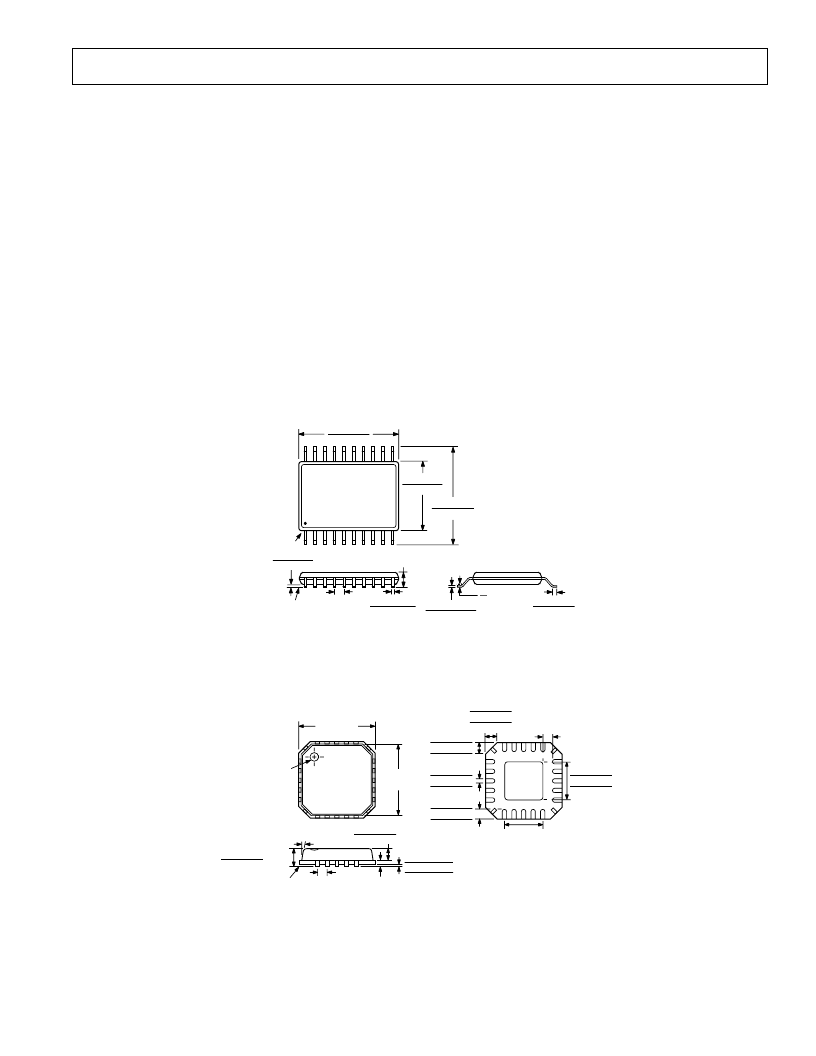
OUTLINE DIMENSIONS
Dimensions shown in inches and (mm).
Thin Shrink Small Outline Package (TSSOP)
(RU-20)
20
11
10
1
0.256 (6.50)
0.246 (6.25)
0.177 (4.50)
0.169 (4.30)
PIN 1
0.006 (0.15)
0.002 (0.05)
0.260 (6.60)
0.252 (6.40)
SEATING
PLANE
0.0118 (0.30)
0.0075 (0.19)
0.0256 (0.65)
BSC
0.0433 (1.10)
MAX
0.0079 (0.20)
0.0035 (0.090)
0.028 (0.70)
0.020 (0.50)
8
0
Chip Scale Package
(CP-20)
1
20
5
6
11
16
15
BVIEW
10
0.080 (2.25)
0.083 (2.10) SQ
0.077 (1.95)
0.024 (0.60)
0.017 (0.42)
0.009 (0.24)
0.024 (0.60)
0.017 (0.42)
0.009 (0.24)
0.012 (0.30)
0.009 (0.23)
0.007 (0.18)
0.030 (0.75)
0.022 (0.60)
0.014 (0.50)
0.080 (2.00)
REF
0.010 (0.25)
MIN
0.020 (0.50)
BSC
12
MAX
0.008 (0.20)
REF
0.031 (0.80) MAX
0.026 (0.65) NOM
0.002 (0.05)
0.0004 (0.01)
0.0 (0.0)
0.035 (0.90) MAX
0.033 (0.85) NOM
SEATING
PLANE
CONTROLLING DIMENSIONS ARE IN MILLIMETERS
PIN 1
INDICATOR
TOP
0.148 (3.75)
BSC SQ
0.157 (4.0)
BSC SQ
Thermal vias may be used on the printed circuit board thermal
pad to improve thermal performance of the package. If vias are
used, they should be incorporated in the thermal pad at 1.2 mm
grid pitch. The via diameter should be between 0.3 mm and
0.33 mm and the via barrel should be plated with 1 oz. copper
to plug the via. The user should connect the printed circuit
board pad to AGND.
相關PDF資料 |
PDF描述 |
|---|---|
| ADF4211 | Dual RF/IF PLL Frequency Synthesizers |
| ADF4211BCP | Dual RF/IF PLL Frequency Synthesizers |
| ADF4211BRU | Dual RF/IF PLL Frequency Synthesizers |
| ADF4212BCP | Dual RF/IF PLL Frequency Synthesizers |
| ADF4212BRU | Dual RF/IF PLL Frequency Synthesizers |
相關代理商/技術參數(shù) |
參數(shù)描述 |
|---|---|
| ADF4211 | 制造商:AD 制造商全稱:Analog Devices 功能描述:Dual RF/IF PLL Frequency Synthesizers |
| ADF4211BCP | 制造商:Rochester Electronics LLC 功能描述:- Bulk |
| ADF4211BRU | 制造商:AD 制造商全稱:Analog Devices 功能描述:Dual RF/IF PLL Frequency Synthesizers |
| ADF4212 | 制造商:AD 制造商全稱:Analog Devices 功能描述:Dual RF/IF PLL Frequency Synthesizers |
| ADF4212BCP | 制造商:Analog Devices 功能描述:PLL FREQ SYNTHESIZER DUAL UP TO 200MHZ 20LFCSP EP - Bulk |
發(fā)布緊急采購,3分鐘左右您將得到回復。