- 您現(xiàn)在的位置:買賣IC網(wǎng) > PDF目錄373983 > ADF4217BRU (ANALOG DEVICES INC) Dual RF PLL Frequency Synthesizers PDF資料下載
參數(shù)資料
| 型號(hào): | ADF4217BRU |
| 廠商: | ANALOG DEVICES INC |
| 元件分類: | XO, clock |
| 英文描述: | Dual RF PLL Frequency Synthesizers |
| 中文描述: | PLL FREQUENCY SYNTHESIZER, 2000 MHz, PDSO20 |
| 封裝: | TSSOP-20 |
| 文件頁(yè)數(shù): | 19/20頁(yè) |
| 文件大小: | 227K |
| 代理商: | ADF4217BRU |
第1頁(yè)第2頁(yè)第3頁(yè)第4頁(yè)第5頁(yè)第6頁(yè)第7頁(yè)第8頁(yè)第9頁(yè)第10頁(yè)第11頁(yè)第12頁(yè)第13頁(yè)第14頁(yè)第15頁(yè)第16頁(yè)第17頁(yè)第18頁(yè)當(dāng)前第19頁(yè)第20頁(yè)
REV. 0
ADF4216/ADF4217/ADF4218
–19–
INTERFACING
The ADF4216/ADF4217/ADF4218 family has a simple SPI-
compatible serial interface for writing to the device. SCLK,
SDATA, and LE (Latch Enable) control the data transfer. When
LE goes high, the 22 bits that have been clocked into the input
register on each rising edge of SCLK will be transferred to the
appropriate latch. See Figure 1 for the Timing Diagram and
Table I for the Latch Truth Table.
The maximum allowable serial clock rate is 20 MHz. This
means that the maximum update rate possible for the device is
909 kHz or one update every 1.1 ms. This is certainly more than
adequate for systems that will have typical lock times in hun-
dreds of microseconds.
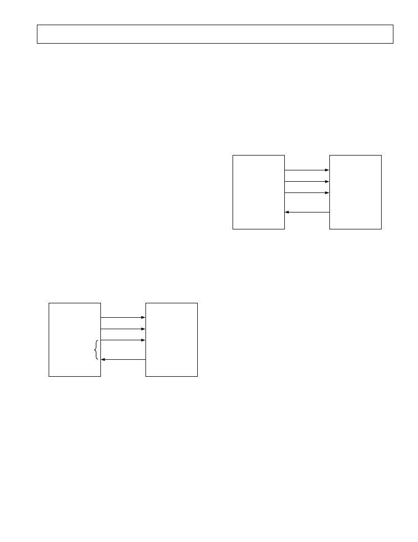
ADuC812 Interface
Figure 9 shows the interface between the ADF421x family and
the ADuC812 microconverter. Since the ADuC812 is based on
an 8051 core, this interface can be used with any 8051-based
microcontroller. The microconverter is set up for SPI Master
Mode with CPHA = 0. To initiate the operation, the I/O port
driving LE is brought low. Each latch of the ADF421x family
needs a 22-bit word. This is accomplished by writing three 8-bit
bytes from the microconverter to the device. When the third
byte has been written, the LE input should be brought high to
complete the transfer.
On first applying power to the ADF421x family, it requires four
writes (one each to the R counter latch and the AB counter latch
for both RF1 and RF2 side) for the output to become active.
When operating in the mode described, the maximum SCLOCK
rate of the ADuC812 is 4 MHz. This means that the maximum
rate at which the output frequency can be changed will be about
180 kHz.
ADuC812
ADF4216/
ADF4217/
ADF4218
SCLK
SDATA
LE
MUXOUT
(LOCK DETECT)
SCLOCK
MOSI
I/O PORTS
Figure 9. ADuC812 to ADF421x Family Interface
ADSP-2181 Interface
Figure 10 shows the interface between the ADF421x family and
the ADSP-21xx Digital Signal Processor. As previously noted,
the ADF421x family needs a 22-bit serial word for each latch
write. The easiest way to accomplish this using the ADSP-21xx
family is to use the Autobuffered Transmit Mode of operation
with Alternate Framing. This provides a means for transmitting
an entire block of serial data before an interrupt is generated.
Set up the word length for eight bits and use three memory
locations for each 22-bit word. To program each 22-bit latch,
store the three 8-bit bytes, enable the Autobuffered mode and
then write to the transmit register of the DSP. This last opera-
tion initiates the autobuffer transfer.
ADSP-21xx
ADF4216/
ADF4217/
ADF4218
SCLK
SDATA
LE
MUXOUT
(LOCK DETECT)
SCLK
DT
I/O FLAG
TFS
Figure 10. ADSP-21xx to ADF421x Family Interface
相關(guān)PDF資料 |
PDF描述 |
|---|---|
| ADF4218 | Dual RF PLL Frequency Synthesizers |
| ADF4218BRU | Dual RF PLL Frequency Synthesizers |
| ADF4251 | Dual Fractional-N/Integer-N Frequency Synthesizer |
| ADF4251BCP | Dual Fractional-N/Integer-N Frequency Synthesizer |
| ADF4251BCP-REEL | Dual Fractional-N/Integer-N Frequency Synthesizer |
相關(guān)代理商/技術(shù)參數(shù) |
參數(shù)描述 |
|---|---|
| ADF4217L | 制造商:未知廠家 制造商全稱:未知廠家 功能描述:ADF4217L/18L/19L: Dual Low Power Frequency Synthesizers Data Sheet (Rev. B. 7/02) |
| ADF4217LBCC | 制造商:Analog Devices 功能描述:PLL Frequency Synthesizer Dual Up to 188MHz 24-Pin LGA |
| ADF4217LBCC-REEL | 制造商:Analog Devices 功能描述:PLL Frequency Synthesizer Dual Up to 188MHz 24-Pin LGA T/R |
| ADF4217LBCC-REEL7 | 制造商:Analog Devices 功能描述:PLL Frequency Synthesizer Dual Up to 188MHz 24-Pin LGA T/R |
| ADF4217LBRU | 制造商:Analog Devices 功能描述:PLL Frequency Synthesizer Dual Up to 188MHz 20-Pin TSSOP |
發(fā)布緊急采購(gòu),3分鐘左右您將得到回復(fù)。