- 您現在的位置:買賣IC網 > PDF目錄373983 > ADF4218 (Analog Devices, Inc.) Dual RF PLL Frequency Synthesizers PDF資料下載
參數資料
| 型號: | ADF4218 |
| 廠商: | Analog Devices, Inc. |
| 元件分類: | XO, clock |
| 英文描述: | Dual RF PLL Frequency Synthesizers |
| 中文描述: | 雙射頻鎖相環頻率合成器 |
| 文件頁數: | 11/20頁 |
| 文件大小: | 227K |
| 代理商: | ADF4218 |
REV. 0
ADF4216/ADF4217/ADF4218
–11–
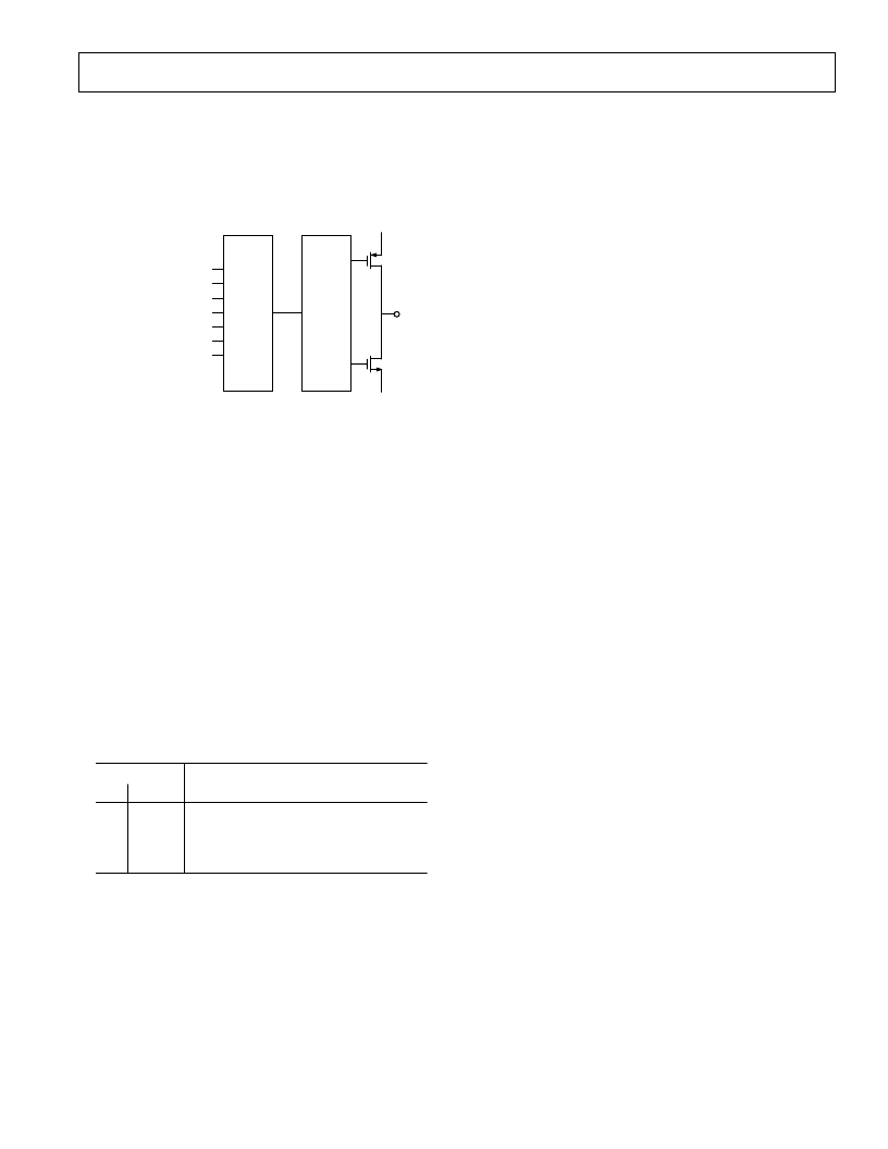
MUXOUT AND LOCK DETECT
The output multiplexer on the ADF4216 family allows the
user to access various internal points on the chip. The state of
MUXOUT is controlled by P3, P4, P11 and P12. See Tables
III and V. Figure 6 shows the MUXOUT section in block dia-
gram form.
CONTROL
MUXOUT
MUX
IF ANALOG LOCK DETECT
IF R COUNTER OUTPUT
IF N COUNTER OUTPUT
IF/RF ANALOG LOCK DETECT
RF R COUNTER OUTPUT
RF N COUNTER OUTPUT
RF ANALOG LOCK DETECT
DGND
DV
DO
Figure 6. MUXOUT Circuit
Lock Detect
MUXOUT can be programmed for analog lock detect. The N-
channel open-drain analog lock detect should be operated with
an external pull-up resistor of 10 k
nominal. When lock has
been detected it is high with narrow low-going pulses.
INPUT SHIFT REGISTER
The functional block diagram for the ADF4216 family is shown
on Page 1. The main blocks include a 22-bit input shift register,
a 14-bit R counter and an 17-bit N counter, comprising a 6-bit
A counter and an 11-bit B counter. Data is clocked into the 22-
bit shift register on each rising edge of CLK. The data is clocked in
MSB first. Data is transferred from the shift register to one of
four latches on the rising edge of LE. The destination latch is
determined by the state of the two control bits (C2, C1) in the
shift register. These are the two LSBs DB1, DB0 as shown in
the timing diagram of Figure 1. The truth table for these bits is
shown in Table I.
Table I. C2, C1 Truth Table
Control Bits
C2
C1
Data Latch
0
0
1
1
0
1
0
1
IF R Counter
IF AB Counter (and Prescaler Select)
RF R Counter
RF AB Counter (and Prescaler Select)
PROGRAM MODES
Table III and Table V show how to set up the Program Modes
in the ADF4216 family. The following should be noted:
1. IF and RF Analog Lock Detect indicate when the PLL is in
lock. When the loop is locked and either IF or RF Analog
Lock Detect is selected, the MUXOUT pin will show a logic
high with narrow low-going pulses. When the IF/RF Analog
Lock Detect is chosen, the locked condition is indicated only
when both IF and RF loops are locked.
2. The IF Counter Reset mode resets the R and N counters in
the IF section and also puts the IF charge pump into three-
state. The RF Counter Reset mode resets the R and N counters
in the RF section and also puts the RF charge pump into
three-state. The IF and RF Counter Reset mode does both
of the above.
Upon removal of the reset bits, the N counter resumes counting
in close alignment with the R counter (maximum error is one
prescaler output cycle).
3. The Fastlock mode uses MUXOUT to switch a second loop
filter damping resistor to ground during Fastlock operation.
Activation of Fastlock occurs whenever RF CP Gain in the
RF Reference counter is set to one.
POWER-DOWN
It is possible to program the ADF4216 family for either synchro-
nous or asynchronous power-down on either the IF or RF side.
Synchronous IF Power-Down
Programming a “1” to P7 of the ADF4216 family will initiate a
power-down. If P2 of the ADF4216 family has been set to “0”
(normal operation), a synchronous power-down is conducted.
The device will automatically put the charge pump into three-
State and then complete the power-down.
Asynchronous IF Power-Down
If P2 of the ADF4216 family has been set to “1” (three-state the
IF charge pump), and P7 is subsequently set to “1,” then an
asynchronous power-down is conducted. The device will go into
power-down on the rising edge of LE, which latches the “1” to
the IF power-down bit (P7).
Synchronous RF Power-Down
Programming a “1” to P16 of the ADF4216 family will initiate a
power-down. If P10 of the ADF4216 family has been set to “0”
(normal operation), a synchronous power-down is conducted. The
device will automatically put the charge pump into three-state
and then complete the power-down.
Asynchronous RF Power-Down
If P10 of the ADF4216 families has been set to “1” (three-state
the RF charge pump), and P16 is subsequently set to “1,” an
asynchronous power-down is conducted. The device will go into
power-down on the rising edge of LE, which latches the “1” to
the RF power-down bit (P16).
Activation of either synchronous or asynchronous power-down
forces the IF/RF loop’s R and N dividers to their load state
conditions and the IF/RF input section is debiased to a high
impedance state.
The REF
IN
oscillator circuit is only disabled if both the IF and
RF power-downs are set.
The input register and latches remain active and are capable of
loading and latching data during all the power-down modes.
The IF/RF section of the devices will return to normal powered
up operation immediately upon LE latching a “0” to the appro-
priate power-down bit.
相關PDF資料 |
PDF描述 |
|---|---|
| ADF4218BRU | Dual RF PLL Frequency Synthesizers |
| ADF4251 | Dual Fractional-N/Integer-N Frequency Synthesizer |
| ADF4251BCP | Dual Fractional-N/Integer-N Frequency Synthesizer |
| ADF4251BCP-REEL | Dual Fractional-N/Integer-N Frequency Synthesizer |
| ADF4251BCP-REEL7 | Dual Fractional-N/Integer-N Frequency Synthesizer |
相關代理商/技術參數 |
參數描述 |
|---|---|
| ADF4218BRU | 制造商:Rochester Electronics LLC 功能描述: 制造商:Analog Devices 功能描述: |
| ADF4218BRU-REEL | 制造商:Analog Devices 功能描述:PLL Frequency Synthesizer Dual 20-Pin TSSOP T/R |
| ADF4218L | 制造商:未知廠家 制造商全稱:未知廠家 功能描述:ADF4217L/18L/19L: Dual Low Power Frequency Synthesizers Data Sheet (Rev. B. 7/02) |
| ADF4218LBCC | 制造商:Analog Devices 功能描述:PLL Frequency Synthesizer Dual Up to 188MHz 24-Pin LGA |
| ADF4218LBCC-REEL | 制造商:Analog Devices 功能描述:PLL Frequency Synthesizer Dual Up to 188MHz 24-Pin LGA T/R |
發布緊急采購,3分鐘左右您將得到回復。