- 您現在的位置:買賣IC網 > PDF目錄373987 > ADG453BN (ANALOG DEVICES INC) LC2MOS 5 ohm RON SPST Switches PDF資料下載
參數資料
| 型號: | ADG453BN |
| 廠商: | ANALOG DEVICES INC |
| 元件分類: | 運動控制電子 |
| 英文描述: | LC2MOS 5 ohm RON SPST Switches |
| 中文描述: | QUAD 1-CHANNEL, SGL POLE SGL THROW SWITCH, PDIP16 |
| 封裝: | PLASTIC, MS-001AB, DIP-16 |
| 文件頁數: | 5/12頁 |
| 文件大小: | 161K |
| 代理商: | ADG453BN |
ADG451/ADG452/ADG453
REV. A
–5–
ORDE RING GUIDE
T emperature
Range
–40
°
C to +85
°
C
–40
°
C to +85
°
C
–40
°
C to +85
°
C
–40
°
C to +85
°
C
–40
°
C to +85
°
C
–40
°
C to +85
°
C
Package
Options*
Model
ADG451BN
ADG451BR
ADG452BN
ADG452BR
ADG453BN
ADG453BR
N-16
R-16A
N-16
R-16A
N-16
R-16A
*N = Plastic DIP; R = Small Outline IC (SOIC).
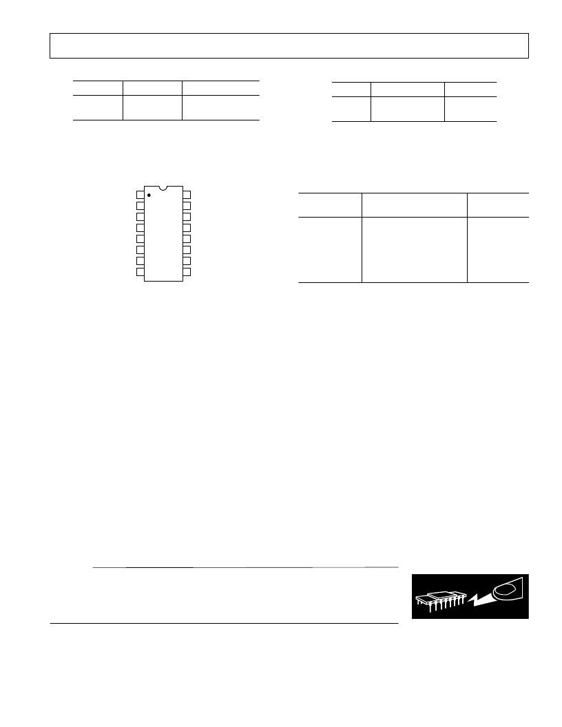
PIN CONFIGURAT ION
(DIP/SOIC)
(TOP VIEW
16
15
14
13
12
11
10
9
1
2
3
4
5
6
7
8
IN1
D1
S1
V
SS
GND
S4
D4
IN4
IN2
D2
S2
V
DD
V
L
S3
D3
IN3
ADG451
ADG452
ADG453
ABSOLUT E MAX IMUM RAT INGS
1
(T
A
= +25
°
C unless otherwise noted)
V
DD
to V
SS
. . . . . . . . . . . . . . . . . . . . . . . . . . . . . . . . . . . .+44 V
V
DD
to GND . . . . . . . . . . . . . . . . . . . . . . . . . . –0.3 V to +25 V
V
SS
to GND . . . . . . . . . . . . . . . . . . . . . . . . . . . +0.3 V to –25 V
V
L
to GND . . . . . . . . . . . . . . . . . . . . . . –0.3 V to V
DD
+ 0.3 V
Analog, Digital Inputs
2
. . . . . . . . . . . V
SS
–2 V to V
DD
+2 V or
30 mA, Whichever Occurs First
Continuous Current, S or D . . . . . . . . . . . . . . . . . . . . 100 mA
Peak Current, S or D . . . . . . . . . . . . . . . . . . . . . . . . . . 300 mA
(Pulsed at 1 ms, 10% Duty Cycle max)
Operating T emperature Range
Industrial (B Version) . . . . . . . . . . . . . . . . . –40
°
C to +85
°
C
Storage T emperature Range . . . . . . . . . . . . . –65
°
C to +150
°
C
Junction T emperature . . . . . . . . . . . . . . . . . . . . . . . . . +150
°
C
Plastic Package, Power Dissipation . . . . . . . . . . . . . . . 470 mW
θ
JA
T hermal Impedance . . . . . . . . . . . . . . . . . . . . . 117
°
C/W
Lead T emperature, Soldering (10 sec) . . . . . . . . . . . +260
°
C
C AUT ION
ESD (electrostatic discharge) sensitive device. Electrostatic charges as high as 4000 V readily
accumulate on the human body and test equipment and can discharge without detection.
Although the ADG451/ADG452/ADG453 feature proprietary ESD protection circuitry, permanent
damage may occur on devices subjected to high energy electrostatic discharges. T herefore, proper ESD
precautions are recommended to avoid performance degradation or loss of functionality.
T ruth T able (ADG453)
Logic
Switch 1, 4
Switch 2, 3
0
1
OFF
ON
ON
OFF
SOIC Package, Power Dissipation . . . . . . . . . . . . . . . . 600 mW
θ
JA
T hermal Impedance . . . . . . . . . . . . . . . . . . . . . . 77
°
C/W
Lead T emperature, Soldering
Vapor Phase (60 sec) . . . . . . . . . . . . . . . . . . . . . . +215
°
C
Infrared (15 sec) . . . . . . . . . . . . . . . . . . . . . . . . . . +220
°
C
ESD . . . . . . . . . . . . . . . . . . . . . . . . . . . . . . . . . . . . . . . . . . 2 kV
NOT ES
1
Stresses above those listed under Absolute Maximum Ratings may cause perma-
nent damage to the device. T his is a stress rating only; functional operation of the
device at these or any other conditions above those listed in the operational
sections of this specification is not implied. Exposure to absolute maximum rating
conditions for extended periods may affect device reliability. Only one absolute
maximum rating may be applied at any one time.
2
Overvoltages at IN, S or D will be clamped by internal diodes. Current should be
limited to the maximum ratings given.
WARNNG
ESD SENSITIVE DEVICE
T ruth T able (ADG451/ADG452)
ADG451 In
ADG452 In
Switch Condition
0
1
1
0
ON
OFF
相關PDF資料 |
PDF描述 |
|---|---|
| ADG453BR | LC2MOS 5 ohm RON SPST Switches |
| ADG465 | Single Channel Protector in an SOT-23 Package |
| ADG465BRM | Single Channel Protector in an SOT-23 Package |
| ADG465BRT | Single Channel Protector in an SOT-23 Package |
| ADG466BR | Triple and Octal Channel Protectors |
相關代理商/技術參數 |
參數描述 |
|---|---|
| ADG453BN | 制造商:Analog Devices 功能描述:SEMICONDUCTORS ((NW)) |
| ADG453BNZ | 功能描述:IC SWITCH QUAD SPST 16DIP RoHS:是 類別:集成電路 (IC) >> 接口 - 模擬開關,多路復用器,多路分解器 系列:LC²MOS 標準包裝:48 系列:- 功能:開關 電路:4 x SPST - NO 導通狀態電阻:100 歐姆 電壓電源:單/雙電源 電壓 - 電源,單路/雙路(±):2 V ~ 12 V,±2 V ~ 6 V 電流 - 電源:50nA 工作溫度:-40°C ~ 85°C 安裝類型:表面貼裝 封裝/外殼:16-SOIC(0.154",3.90mm 寬) 供應商設備封裝:16-SOIC 包裝:管件 |
| ADG453BNZ1 | 制造商:AD 制造商全稱:Analog Devices 功能描述:LC2MOS 5 ?? RON SPST Switches |
| ADG453BR | 功能描述:IC SWITCH QUAD SPST 16SOIC RoHS:否 類別:集成電路 (IC) >> 接口 - 模擬開關,多路復用器,多路分解器 系列:LC²MOS 其它有關文件:STG4159 View All Specifications 標準包裝:5,000 系列:- 功能:開關 電路:1 x SPDT 導通狀態電阻:300 毫歐 電壓電源:雙電源 電壓 - 電源,單路/雙路(±):±1.65 V ~ 4.8 V 電流 - 電源:50nA 工作溫度:-40°C ~ 85°C 安裝類型:表面貼裝 封裝/外殼:7-WFBGA,FCBGA 供應商設備封裝:7-覆晶 包裝:帶卷 (TR) |
| ADG453BR-REEL | 功能描述:IC SWITCH QUAD SPST 16SOIC RoHS:否 類別:集成電路 (IC) >> 接口 - 模擬開關,多路復用器,多路分解器 系列:LC²MOS 標準包裝:48 系列:- 功能:開關 電路:4 x SPST - NO 導通狀態電阻:100 歐姆 電壓電源:單/雙電源 電壓 - 電源,單路/雙路(±):2 V ~ 12 V,±2 V ~ 6 V 電流 - 電源:50nA 工作溫度:-40°C ~ 85°C 安裝類型:表面貼裝 封裝/外殼:16-SOIC(0.154",3.90mm 寬) 供應商設備封裝:16-SOIC 包裝:管件 |
發布緊急采購,3分鐘左右您將得到回復。