- 您現在的位置:買賣IC網 > PDF目錄373987 > ADG508FTQ (ANALOG DEVICES INC) 4/8 Channel Fault-Protected Analog Multiplexers PDF資料下載
參數資料
| 型號: | ADG508FTQ |
| 廠商: | ANALOG DEVICES INC |
| 元件分類: | 運動控制電子 |
| 英文描述: | 4/8 Channel Fault-Protected Analog Multiplexers |
| 中文描述: | 8-CHANNEL, SGL ENDED MULTIPLEXER, CDIP16 |
| 封裝: | CERDIP-16 |
| 文件頁數: | 5/12頁 |
| 文件大小: | 170K |
| 代理商: | ADG508FTQ |
ADG508F/ADG509F/ADG528F
Typical Performance Graphs
REV. C
–5–
TERMINOLOGY
V
DD
V
SS
GND
R
ON
R
ON
Drift
Most positive power supply potential.
Most negative power supply potential.
Ground (0 V) reference.
Ohmic resistance between D and S.
Change in R
ON
when temperature changes
by one degree Celsius.
Difference between the R
ON
of any two
channels.
Source leakage current when the switch is
off.
Drain leakage current when the switch is off.
Channel leakage current when the switch is
on.
Analog voltage on terminals D, S.
Channel input capacitance for “OFF”
condition.
Channel output capacitance for “OFF”
condition.
“ON” switch capacitance.
Digital input capacitance.
Delay time between the 50% and 90% points
of the digital input and switch “ON”
condition.
Delay time between the 50% and 90% points
of the digital input and switch “OFF”
condition.
Delay time between the 50% and 90% points
of the digital inputs and the switch “ON”
condition when switching from one address
state to another.
“OFF” time measured between 80% points of
both switches when switching from one
address state to another.
Maximum input voltage for Logic “0”.
Minimum input voltage for Logic “1”.
Input current of the digital input.
A measure of unwanted signal coupling
through an “OFF” channel.
A measure of the glitch impulse transferred
from the digital input to the analog output
during switching.
Positive supply current.
Negative supply current.
R
ON
Match
I
S
(OFF)
I
D
(OFF)
I
D
, I
S
(ON)
V
D
(V
S
)
C
S
(OFF)
C
D
(OFF)
C
D
, C
S
(ON)
C
IN
t
ON
(EN)
t
OFF
(EN)
t
TRANSITION
t
OPEN
V
INL
V
INH
I
INL
(I
INH
)
Off Isolation
Charge Injection
I
DD
I
SS
2000
1000
0
–15
–5
15
5
0
10
–10
500
1750
1500
1250
750
250
V
D
(V
S
) – Volts
R
O
V
T
A
= +25
8
C
V
DD
= +5V
V
SS
= –5V
V
DD
= +10V
V
SS
= –10V
V
DD
= +15V
V
SS
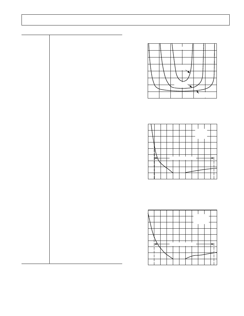
= –15V
Figure 3. On Resistance as a Function of V
D
(V
S
)
1m
1
m
1p
–50
–30
50
10
–20
V
IN
– INPUT VOLTAGE – Volts
20
–40
1n
30
40
100
m
10
m
10n
100n
10p
100p
–10
0
I
S
V
DD
= 0V
V
SS
= 0V
V
D
= 0V
60
OPERATING RANGE
Figure 4. Input Leakage Current as a Function of V
S
(Power Supplies OFF) During Overvoltage Conditions
1m
1
m
1p–50
–30
50
10
–20
V
IN
– INPUT VOLTAGE – Volts
20
–40
1n
30
40
100
m
10
m
10n
100n
10p
100p
–10
0
I
D
V
DD
= +15V
V
SS
= –15V
V
D
= 0V
60
OPERATING RANGE
Figure 5. Output Leakage Current as a Function of V
S
(Power Supplies ON) During Overvoltage Conditions
相關PDF資料 |
PDF描述 |
|---|---|
| ADG509AKP | CMOS 4/8 CHAANNEL ANALOG MULTIPLEXERS |
| ADG509AKR | CMOS 4/8 CHAANNEL ANALOG MULTIPLEXERS |
| ADG509ATE | CMOS 4/8 CHAANNEL ANALOG MULTIPLEXERS |
| ADG509ATQ | CMOS 4/8 CHAANNEL ANALOG MULTIPLEXERS |
| ADG528FTQ | 4/8 Channel Fault-Protected Analog Multiplexers |
相關代理商/技術參數 |
參數描述 |
|---|---|
| ADG508FTQ/883B | 制造商:未知廠家 制造商全稱:未知廠家 功能描述:8-Channel Analog Multiplexer |
| ADG509A | 制造商:未知廠家 制造商全稱:未知廠家 功能描述:CMOS 4/8 Channel Analog Multiplexers |
| ADG509ABCHIPS | 制造商:未知廠家 制造商全稱:未知廠家 功能描述:4-Channel Analog Multiplexer |
| ADG509ABQ | 功能描述:IC MULTIPLEXER DUAL 4X1 16CDIP RoHS:否 類別:集成電路 (IC) >> 接口 - 模擬開關,多路復用器,多路分解器 系列:- 標準包裝:48 系列:- 功能:開關 電路:4 x SPST - NO 導通狀態電阻:100 歐姆 電壓電源:單/雙電源 電壓 - 電源,單路/雙路(±):2 V ~ 12 V,±2 V ~ 6 V 電流 - 電源:50nA 工作溫度:-40°C ~ 85°C 安裝類型:表面貼裝 封裝/外殼:16-SOIC(0.154",3.90mm 寬) 供應商設備封裝:16-SOIC 包裝:管件 |
| ADG509AKN | 功能描述:IC MULTIPLEXER DUAL 4X1 16DIP RoHS:否 類別:集成電路 (IC) >> 接口 - 模擬開關,多路復用器,多路分解器 系列:- 其它有關文件:STG4159 View All Specifications 標準包裝:5,000 系列:- 功能:開關 電路:1 x SPDT 導通狀態電阻:300 毫歐 電壓電源:雙電源 電壓 - 電源,單路/雙路(±):±1.65 V ~ 4.8 V 電流 - 電源:50nA 工作溫度:-40°C ~ 85°C 安裝類型:表面貼裝 封裝/外殼:7-WFBGA,FCBGA 供應商設備封裝:7-覆晶 包裝:帶卷 (TR) |
發布緊急采購,3分鐘左右您將得到回復。