- 您現在的位置:買賣IC網 > PDF目錄373988 > ADG513BN (ANALOG DEVICES INC) LC2MOS Precision 5 V/3 V Quad SPST Switches PDF資料下載
參數資料
| 型號: | ADG513BN |
| 廠商: | ANALOG DEVICES INC |
| 元件分類: | 運動控制電子 |
| 英文描述: | LC2MOS Precision 5 V/3 V Quad SPST Switches |
| 中文描述: | QUAD 1-CHANNEL, SGL POLE SGL THROW SWITCH, PDIP16 |
| 封裝: | PLASTIC, DIP-16 |
| 文件頁數: | 8/11頁 |
| 文件大小: | 124K |
| 代理商: | ADG513BN |
ADG511/ADG512/ADG513
REV. B
–8–
V
D
OR V
S
– DRAIN OR SOURCE VOLTAGE – V
0.008
0.000
–0.006
–5
5
–4
L
–3
–2
–1
0
1
2
3
4
0.004
0.002
–0.002
–0.004
V
DD
= +5V
V
SS
= –5V
T
A
= +25
8
C
I
D
(OFF)
I
D
(ON)
I
S
(OFF)
Figure 7. Leakage Currents as a Function of V
D
(V
S
)
FREQUENCY – Hz
110
100
60100
10M
1k
C
10k
100k
1M
90
80
70
V
DD
= +5V
V
SS
= –5V
Figure 8. Crosstalk vs. Frequency
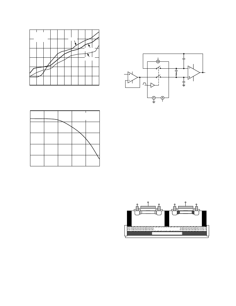
APPLICATION
Figure 9 illustrates a precise sample-and-hold circuit. An AD845
is used as the input buffer while the output operational amplifier
is an OP07. During the track mode, SW1 is closed and the
output V
OUT
follows the input signal V
IN
. In the hold mode,
SW1 is opened and the signal is held by the hold capacitor C
H
.
Due to switch and capacitor leakage, the voltage on the hold
capacitor will decrease with time. The ADG511/ADG512/
ADG513 minimizes this droop due to its low leakage specifica-
tions. The droop rate is further minimized by the use of a poly-
styrene hold capacitor. The droop rate for the circuit shown is
typically 15
μ
V/
μ
s.
A second switch, SW2, which operates in parallel with SW1, is
included in this circuit to reduce pedestal error. Since both
switches will be at the same potential, they will have a differen-
tial effect on the op amp OP07, which will minimize charge
injection effects. Pedestal error is also reduced by the compensation
network R
C
and C
C
. This compensation network also reduces
the hold time glitch while optimizing the acquisition time. Using
the illustrated op amps and component values, the pedestal
error has a maximum value of 5 mV over the
±
3 V input range.
The acquisition time is 2.5
μ
s while the settling time is 1.85
μ
s.
+5V
–5V
2200pF
R
C
75
V
C
1000pF
C
H
2200pF
V
OUT
ADG511
ADG512
ADG513
SW1
SW2
S
S
D
D
+5V
–5V
AD845
+5V
–5V
V
IN
OP07
Figure 9. Accurate Sample-and-Hold
TRENCH ISOLATION
The MOS devices that make up the ADG511A/ADG512A/
ADG513A are isolated from each other by an oxide layer
(trench) (see Figure 10). When the NMOS and PMOS devices
are not electrically isolated from each other, there exists the
possibility of “latch-up” caused by parasitic junctions between
CMOS transistors. Latch-up is caused when P-N junctions that
are normally reverse biased, become forward biased, causing
large currents to flow. This can be destructive.
CMOS devices are normally isolated from each other by
Junction Isolation
. In Junction Isolation the N and P wells of the
CMOS transistors form a diode that is reverse biased under
normal operation. However, during overvoltage conditions, this
diode becomes forward biased. A Silicon-Controlled Rectifier
(SCR)-type circuit is formed by the two transistors, causing a
significant amplification of the current that, in turn, leads to
latch-up. With Trench Isolation, this diode is removed; the
result is a latch-up-proof circuit.
BURIED OXIDE LAYER
SUBSTRATE (BACKGATE)
T
R
E
N
C
H
T
R
E
N
C
H
T
R
E
N
C
H
P
+
P
+
P-CHANNEL
N
+
N
+
N-CHANNEL
P
–
N
–
V
G
V
D
V
S
V
G
V
D
V
S
Figure 10. Trench Isolation
相關PDF資料 |
PDF描述 |
|---|---|
| ADG513BR | LC2MOS Precision 5 V/3 V Quad SPST Switches |
| ADG526 | CMOS LATCHED 8/16 CHANNEL ANALOG MULTIPLEXERS |
| ADG526A | CMOS LATCHED 8/16 CHANNEL ANALOG MULTIPLEXERS |
| ADG526A-527A | LATCHED 8/16 CHANNEL ANALOG MULTIPLEXERS |
| ADG526ABQ | CMOS LATCHED 8/16 CHANNEL ANALOG MULTIPLEXERS |
相關代理商/技術參數 |
參數描述 |
|---|---|
| ADG513BNZ | 功能描述:IC SWITCH QUAD SPST 16DIP RoHS:是 類別:集成電路 (IC) >> 接口 - 模擬開關,多路復用器,多路分解器 系列:LC²MOS 其它有關文件:STG4159 View All Specifications 標準包裝:5,000 系列:- 功能:開關 電路:1 x SPDT 導通狀態電阻:300 毫歐 電壓電源:雙電源 電壓 - 電源,單路/雙路(±):±1.65 V ~ 4.8 V 電流 - 電源:50nA 工作溫度:-40°C ~ 85°C 安裝類型:表面貼裝 封裝/外殼:7-WFBGA,FCBGA 供應商設備封裝:7-覆晶 包裝:帶卷 (TR) |
| ADG513BR | 制造商:Analog Devices 功能描述:Analog Switch Quad SPST 16-Pin SOIC N 制造商:Analog Devices 功能描述:IC SWITCH SPST QUAD CMOS |
| ADG513BR-REEL | 制造商:Analog Devices 功能描述:Analog Switch Quad SPST 16-Pin SOIC N T/R |
| ADG513BR-REEL7 | 制造商:Analog Devices 功能描述:Analog Switch Quad SPST 16-Pin SOIC N T/R |
| ADG513BRZ | 功能描述:IC SWITCH QUAD SPST 16SOIC RoHS:是 類別:集成電路 (IC) >> 接口 - 模擬開關,多路復用器,多路分解器 系列:LC²MOS 其它有關文件:STG4159 View All Specifications 標準包裝:5,000 系列:- 功能:開關 電路:1 x SPDT 導通狀態電阻:300 毫歐 電壓電源:雙電源 電壓 - 電源,單路/雙路(±):±1.65 V ~ 4.8 V 電流 - 電源:50nA 工作溫度:-40°C ~ 85°C 安裝類型:表面貼裝 封裝/外殼:7-WFBGA,FCBGA 供應商設備封裝:7-覆晶 包裝:帶卷 (TR) |
發布緊急采購,3分鐘左右您將得到回復。