- 您現在的位置:買賣IC網 > PDF目錄373989 > ADG619BRT (ANALOG DEVICES INC) CMOS +-5 V/ +5V 4 OHM SINGLE SPDT SWITCHES PDF資料下載
參數資料
| 型號: | ADG619BRT |
| 廠商: | ANALOG DEVICES INC |
| 元件分類: | 運動控制電子 |
| 英文描述: | CMOS +-5 V/ +5V 4 OHM SINGLE SPDT SWITCHES |
| 中文描述: | 2-CHANNEL, SGL POLE DOUBLE THROW SWITCH, PDSO8 |
| 封裝: | PLASTIC, SOT-23, 8 PIN |
| 文件頁數: | 5/8頁 |
| 文件大小: | 145K |
| 代理商: | ADG619BRT |
REV. 0
–5–
ADG619/ADG620
TERMINOLOGY
Mnemonic
Description
V
DD
V
SS
Most Positive Power Supply Potential
Most Negative Power Supply in a Dual Supply Application. In single supply applications, this should be
tied to ground at the device.
Ground (0 V) Reference
Positive Supply Current
Negative Supply Current
Source Terminal. May be an input or output.
Drain Terminal. May be an input or output.
Logic Control Input
Ohmic Resistance Between D and S
On Resistance Match Between Any Two Channels, i.e., R
ON
Max – R
ON
Min.
Flatness is Defined as the Difference Between the Maximum and Minimum Value of On Resistance as
Measured Over the Specified Analog Signal Range.
Source Leakage Current With the Switch “OFF”
Channel Leakage Current With the Switch “ON”
Analog Voltage on Terminals D, S
Maximum Input Voltage for Logic “0”
Minimum Input Voltage for Logic “1”
Input Current of the Digital Input
“OFF” Switch Source Capacitance
“ON” Switch Capacitance
Delay Between Applying the Digital Control Input and the Output Switching On
Delay Between Applying the Digital Control Input and the Output Switching Off
“ON” Time, Measured Between the 80% Points of Both Switches, When Switching From One Address
State to Another
“OFF” Time or “ON” Time Measured Between the 90% Points of Both Switches, When Switching from
One Address State to Another
A Measure of the Glitch Impulse Transfered From the Digital Input to the Analog Output During Switching
A Measure of Unwanted Signal that is Coupled Through From One Channel to Another as a Result of
Parasitic Capacitance
A Measure of Unwanted Signal Coupling Through an “OFF” Switch
The Frequency Response of the “ON” Switch
The Loss Due to the ON Resistance of the Switch
GND
I
DD
I
SS
S
D
IN
R
ON
DR
ON
R
FLAT(ON)
I
S
(OFF)
I
D
, I
S
(ON)
V
D
(V
S
)
V
INL
V
INH
I
INL
(I
INH
)
C
S
(OFF)
C
D
, C
S
(ON)
t
ON
t
OFF
t
MBB
t
BBM
Charge Injection
Crosstalk
Off Isolation
Bandwidth
Insertion Loss
V
D
, V
S
– V
–3
5
1
3
O
8
0
3
2
5
–5
–1
7
1
6
4
–2
2
4
–4
0
T
A
= 25 C
V
DD
, V
SS
= 2.5V
V
DD
, V
SS
= 3V
V
DD
, V
SS
= 3.3V
V
DD
, V
SS
= 4.5V
V
DD
, V
SS
= 5V
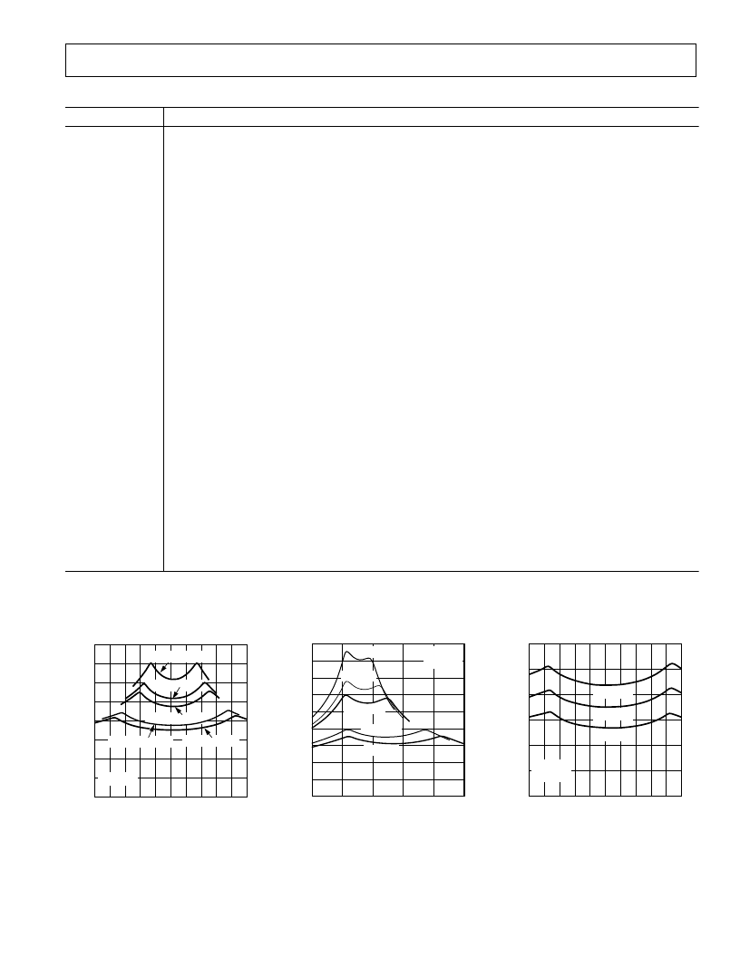
TPC 1. On Resistance vs. V
D
(V
S
)
–
Dual Supply
Typical Performance Characteristics
V
D
, V
S
–
V
1
5
3
4
O
–
18
0
4
14
10
0
2
16
6
2
12
8
T
A
= 25 C
V
SS
= 0V
V
DD
= 2.7V
V
DD
= 3V
V
DD
= 3.3V
V
DD
= 4.5V
V
DD
= 5V
TPC 2. On Resistance vs. V
D
(V
S
)
–
Single Supply
V
D
, V
S
–
V
–
3
5
1
3
O
–
6
0
1
5
–
5
–
1
2
4
3
–
2
2
4
–
4
0
T
A
= +85 C
T
A
= +25 C
T
A
=
–
40 C
V
DD
= +5V
V
SS
=
–
5V
TPC 3. On Resistance vs. V
D
(V
S
) for
Different Temperatures
–
Dual Supply
相關PDF資料 |
PDF描述 |
|---|---|
| ADG620 | CMOS +-5 V/ +5V 4 OHM SINGLE SPDT SWITCHES |
| ADG621BRM | CMOS +-5 V/ +5V 4 OHM DUAL SPST SWITCHES |
| ADG622 | CMOS +-5 V/ +5V 4 OHM DUAL SPST SWITCHES |
| ADG622BRM | CMOS +-5 V/ +5V 4 OHM DUAL SPST SWITCHES |
| ADG623 | CMOS +-5 V/ +5V 4 OHM DUAL SPST SWITCHES |
相關代理商/技術參數 |
參數描述 |
|---|---|
| ADG619BRT-500RL7 | 制造商:Analog Devices 功能描述:Analog Switch Single SPDT 8-Pin SOT-23 T/R 制造商:Analog Devices 功能描述:IC SWITCH SPDT CMOS |
| ADG619BRT-R2 | 制造商:Analog Devices 功能描述: |
| ADG619BRT-REEL | 制造商:AD 制造商全稱:Analog Devices 功能描述:CMOS, ?±5 V/5 V, 4 ??, Single SPDT Switches |
| ADG619BRT-REEL7 | 制造商:Analog Devices 功能描述: 制造商:Rochester Electronics LLC 功能描述: |
| ADG619BRTZ-500RL7 | 功能描述:IC SWITCH SPDT SOT23-8 RoHS:是 類別:集成電路 (IC) >> 接口 - 模擬開關,多路復用器,多路分解器 系列:- 標準包裝:1,000 系列:- 功能:多路復用器 電路:1 x 4:1 導通狀態電阻:- 電壓電源:雙電源 電壓 - 電源,單路/雙路(±):±5V 電流 - 電源:7mA 工作溫度:-40°C ~ 85°C 安裝類型:表面貼裝 封裝/外殼:16-SOIC(0.154",3.90mm 寬) 供應商設備封裝:16-SOIC 包裝:帶卷 (TR) |
發布緊急采購,3分鐘左右您將得到回復。