- 您現在的位置:買賣IC網 > PDF目錄373991 > ADG774BR (ANALOG DEVICES INC) CMOS 3 V/5 V, Wide Bandwidth Quad 2:1 Mux PDF資料下載
參數資料
| 型號: | ADG774BR |
| 廠商: | ANALOG DEVICES INC |
| 元件分類: | 運動控制電子 |
| 英文描述: | CMOS 3 V/5 V, Wide Bandwidth Quad 2:1 Mux |
| 中文描述: | QUAD 2-CHANNEL, SGL ENDED MULTIPLEXER, PDSO16 |
| 封裝: | MS-012AC, SOIC-16 |
| 文件頁數: | 4/8頁 |
| 文件大小: | 119K |
| 代理商: | ADG774BR |
ADG774
–4–
REV. 0
ORDERING GUIDE
Model
Temperature Range
–40
°
C to +85
°
C
–40
°
C to +85
°
C
Package Descriptions
Package Options
ADG774BR
ADG774BRQ
R = 0.15" Small Outline IC (SOIC)
RQ = 0.15" Quarter Size Outline Package (QSOP)
R-16A
RQ-16
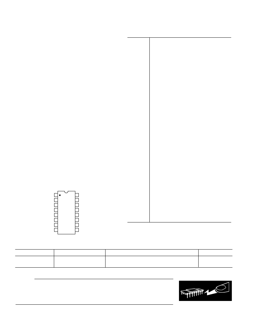
PIN CONFIGURATION
(SOIC/QSOP)
TOP VIEW
(Not to Scale)
16
15
14
13
12
11
10
9
1
2
3
4
5
6
7
8
IN
S1A
S1B
D1
S2A
S2B
D2
GND
V
DD
EN
S4A
S4B
D4
S3A
S3B
D3
ADG774
CAUTION
ESD (electrostatic discharge) sensitive device. Electrostatic charges as high as 4000 V readily
accumulate on the human body and test equipment and can discharge without detection.
Although the ADG774 features proprietary ESD protection circuitry, permanent damage may
occur on devices subjected to high energy electrostatic discharges. Therefore, proper ESD
precautions are recommended to avoid performance degradation or loss of functionality.
WARNING!
ESD SENSITIVE DEVICE
ABSOLUTE MAXIMUM RATINGS
1
(T
A
= +25
°
C unless otherwise noted)
V
DD
to GND . . . . . . . . . . . . . . . . . . . . . . . . . . . –0.3 V to +6 V
Analog, Digital Inputs
2
. . . . . . . . . . . –0.3 V to V
DD
+ 0.3 V or
30 mA, Whichever Occurs First
Continuous Current, S or D . . . . . . . . . . . . . . . . . . . . 100 mA
Peak Current, S or D . . . . . . . . . . . . . . . . . . . . . . . . . 300 mA
(Pulsed at 1 ms, 10% Duty Cycle max)
Operating Temperature Range
Industrial (B Version) . . . . . . . . . . . . . . . . . –40
°
C to +85
°
C
Storage Temperature Range . . . . . . . . . . . . . –65
°
C to +150
°
C
Junction Temperature . . . . . . . . . . . . . . . . . . . . . . . . . +150
°
C
SOIC Package, Power Dissipation . . . . . . . . . . . . . . . . 600 mW
θ
JA
Thermal Impedance . . . . . . . . . . . . . . . . . . . . . 100
°
C/W
Lead Temperature, Soldering
Vapor Phase (60 sec) . . . . . . . . . . . . . . . . . . . . . . . . +215
°
C
Infrared (15 sec) . . . . . . . . . . . . . . . . . . . . . . . . . . . . +220
°
C
QSOP Package, Power Dissipation . . . . . . . . . . . . . . . 566 mW
θ
JA
Thermal Impedance . . . . . . . . . . . . . . . . . . . 149.97
°
C/W
Lead Temperature, Soldering
Vapor Phase (60 sec) . . . . . . . . . . . . . . . . . . . . . . . . +215
°
C
Infrared (15 sec) . . . . . . . . . . . . . . . . . . . . . . . . . . . . +220
°
C
ESD . . . . . . . . . . . . . . . . . . . . . . . . . . . . . . . . . . . . . . . . . . 2 kV
NOTES
1
Stresses above those listed under Absolute Maximum Ratings may cause perma-
nent damage to the device. This is a stress rating only; functional operation of the
device at these or any other conditions above those listed in the operational sections
of this specification is not implied. Exposure to absolute maximum rating condi-
tions for extended periods may affect device reliability. Only one absolute maxi-
mum rating may be applied at any one time.
2
Overvoltages at IN, S or D will be clamped by internal diodes. Current should be
limited to the maximum ratings given.
TERMINOLOGY
V
DD
GND
S
D
IN
EN
R
ON
R
ON
Most Positive Power Supply Potential.
Ground (0 V) Reference.
Source Terminal. May be an input or output.
Drain Terminal. May be an input or output.
Logic Control Input.
Logic Control Input.
Ohmic resistance between D and S.
On Resistance match between any two channels
i.e., R
ON
max – R
ON
min.
Flatness is defined as the difference between the
maximum and minimum value of on resistance
as measured over the specified analog signal
range.
Source Leakage Current with the switch “OFF.”
Drain Leakage Current with the switch “OFF.”
Channel Leakage Current with the switch “ON.”
Analog Voltage on Terminals D, S.
“OFF” Switch Source Capacitance.
“OFF” Switch Drain Capacitance.
C
D
, C
S
(ON) “ON” Switch Capacitance.
t
ON
Delay between applying the digital control input
and the output switching on. See Test Circuit 4.
t
OFF
Delay between applying the digital control input
and the output switching Off.
t
D
“OFF” time or “ON” time measured between
the 90% points of both switches, when switching
from one address state to another. See Test
Circuit 5.
Crosstalk
A measure of unwanted signal that is coupled
through from one channel to another as a result
of parasitic capacitance.
Off Isolation A measure of unwanted signal coupling through an
“OFF” switch.
Bandwidth
Frequency response of the switch in the ON
state measured at 3 dB down.
Distortion
R
FLAT(ON)
/R
L
R
FLAT(ON)
I
S
(OFF)
I
D
(OFF)
I
D
, I
S
(ON)
V
D
(V
S
)
C
S
(OFF)
C
D
(OFF)
相關PDF資料 |
PDF描述 |
|---|---|
| ADG774BRQ | CMOS 3 V/5 V, Wide Bandwidth Quad 2:1 Mux |
| ADG774ABRQ | Low Voltage 400 MHz Quad 2:1 Mux with 3 ns Switching Time |
| ADG779BKS | CMOS 1.8 V to 5.5 V, 2.5 ohm SPDT Switch/2:1 Mux In Tiny SC70 Package |
| ADG779 | CMOS 1.8 V to 5.5 V, 2.5 ohm SPDT Switch/2:1 Mux In Tiny SC70 Package |
| ADG781 | 2.5 ohm Quad SPST Switches in Chip Scale Package |
相關代理商/技術參數 |
參數描述 |
|---|---|
| ADG774BRQ | 功能描述:IC MUX/DEMUX QUAD 2X1 16QSOP RoHS:否 類別:集成電路 (IC) >> 接口 - 模擬開關,多路復用器,多路分解器 系列:- 標準包裝:48 系列:- 功能:開關 電路:4 x SPST - NO 導通狀態電阻:100 歐姆 電壓電源:單/雙電源 電壓 - 電源,單路/雙路(±):2 V ~ 12 V,±2 V ~ 6 V 電流 - 電源:50nA 工作溫度:-40°C ~ 85°C 安裝類型:表面貼裝 封裝/外殼:16-SOIC(0.154",3.90mm 寬) 供應商設備封裝:16-SOIC 包裝:管件 |
| ADG774BRQ-500RL7 | 功能描述:4 Circuit IC Switch 2:1 2.2 Ohm (Typ) 16-QSOP 制造商:analog devices inc. 系列:- 包裝:帶卷(TR) 零件狀態:上次購買時間 開關電路:SPDT 多路復用器/解復用器電路:2:1 電路數:4 導通電阻(最大值):2.2 歐姆(標準) 通道至通道匹配(ΔRon):150 毫歐 電壓 -?電源,單(V+):3 V ~ 5 V 電壓 - 電源,雙(V±):- 開關時間(Ton, Tof)(最大值):15ns,8ns -3db 帶寬:240MHz 電荷注入:10pC 溝道電容 (CS(off),CD(off)):10pF,20pF 電流 - 漏泄(IS(off))(最大值):500pA 串擾:-75dB @ 10MHz 工作溫度:-40°C ~ 125°C(TA) 封裝/外殼:16-SSOP(0.154",3.90mm 寬) 供應商器件封裝:16-QSOP 標準包裝:1 |
| ADG774BRQ-REEL | 功能描述:IC MUX/DEMUX QUAD 2X1 16QSOP RoHS:否 類別:集成電路 (IC) >> 接口 - 模擬開關,多路復用器,多路分解器 系列:- 標準包裝:48 系列:- 功能:開關 電路:4 x SPST - NO 導通狀態電阻:100 歐姆 電壓電源:單/雙電源 電壓 - 電源,單路/雙路(±):2 V ~ 12 V,±2 V ~ 6 V 電流 - 電源:50nA 工作溫度:-40°C ~ 85°C 安裝類型:表面貼裝 封裝/外殼:16-SOIC(0.154",3.90mm 寬) 供應商設備封裝:16-SOIC 包裝:管件 |
| ADG774BRQ-REEL7 | 功能描述:IC MUX/DEMUX QUAD 2X1 16QSOP RoHS:否 類別:集成電路 (IC) >> 接口 - 模擬開關,多路復用器,多路分解器 系列:- 標準包裝:1,000 系列:- 功能:多路復用器 電路:1 x 4:1 導通狀態電阻:- 電壓電源:雙電源 電壓 - 電源,單路/雙路(±):±5V 電流 - 電源:7mA 工作溫度:-40°C ~ 85°C 安裝類型:表面貼裝 封裝/外殼:16-SOIC(0.154",3.90mm 寬) 供應商設備封裝:16-SOIC 包裝:帶卷 (TR) |
| ADG774BRQZ | 功能描述:IC MUX/DEMUX QUAD 2X1 16QSOP RoHS:是 類別:集成電路 (IC) >> 接口 - 模擬開關,多路復用器,多路分解器 系列:- 特色產品:MicroPak? 標準包裝:1 系列:- 功能:開關 電路:2 x SPST - NC 導通狀態電阻:500 毫歐 電壓電源:單電源 電壓 - 電源,單路/雙路(±):1.4 V ~ 4.3 V 電流 - 電源:150nA 工作溫度:-40°C ~ 125°C 安裝類型:表面貼裝 封裝/外殼:8-XFDFN 供應商設備封裝:8-XSON,SOT833-1 (1.95x1) 包裝:Digi-Reel® 其它名稱:568-5557-6 |
發布緊急采購,3分鐘左右您將得到回復。