- 您現在的位置:買賣IC網 > PDF目錄373994 > ADL5542 (Analog Devices, Inc.) 50 MHz to 6 GHz RF/IF Gain Block PDF資料下載
參數資料
| 型號: | ADL5542 |
| 廠商: | Analog Devices, Inc. |
| 英文描述: | 50 MHz to 6 GHz RF/IF Gain Block |
| 中文描述: | 50 MHz至6 GHz的射頻/中頻增益模塊 |
| 文件頁數: | 10/12頁 |
| 文件大小: | 193K |
| 代理商: | ADL5542 |
ADL5542
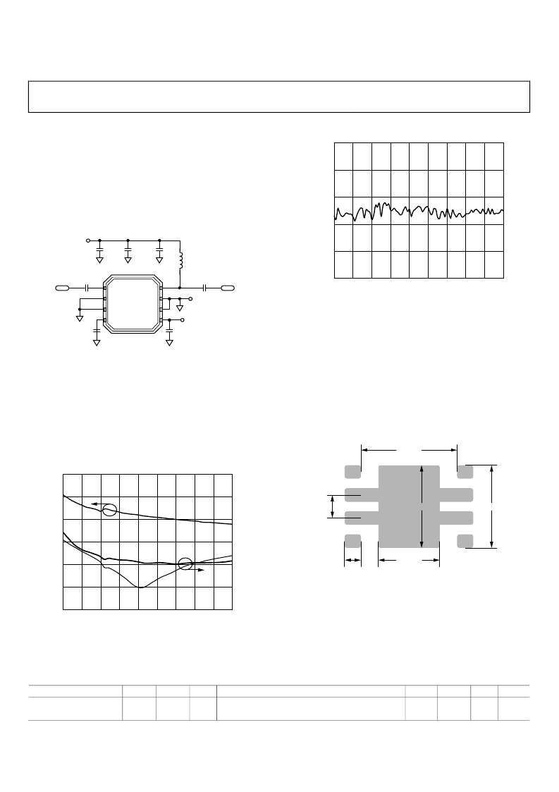
BASIC CONNECTIONS
The basic connections for operating the ADL5542 are shown in
Figure 13. Recommended components are listed in Table 5. The
input and output should be ac-coupled with appropriately sized
capacitors (device characterization was performed with 33 pF
capacitors). A 5 V dc bias is supplied to the amplifier via VPOS
(Pin 5) and through a biasing inductor connected to RFOUT
(Pin 8). The bias voltage should be decoupled using a 1 μF
capacitor, a 1.2 nF capacitor, and two 68 pF capacitors.
Rev. A | Page 10 of 12
4.0
1.5
50
500
FREQUENCY (MHz)
N
3.5
3.0
2.5
2.0
VCC
3 GND
6
GND
4 CB
5
VPOS
1 RFIN
8
RFOUT
2 GND
7
GND
ADL5542
C4
68pF
C5
1.2nF
C6
1μF
VCC
C2
33pF
C1
33pF
RFIN
RFOUT
L1
47nH
C3
1μF
100
150
200
250
300
350
400
450
0
GND
C7
68pF
0
50
500
FREQUENCY (MHz)
0
Figure 13. Basic Connections
For operation between 50 MHz and 500 MHz, a larger biasing
choke and ac coupling capacitors are necessary (see Table 5).
Figure 14 shows a plot of the input return loss, the output
return loss, and the gain with these components. At 100 MHz,
the ADL5542 achieves an OIP3 of 38 dBm (P
OUT
= 0 dBm per
tone). The noise figure performance for operation from 50 MHz
to 500 MHz is shown in Figure 15. When operating below
50 MHz, the ADL5542 exhibits gain peaking, and the input
and output match degrade significantly.
21.0
18.0
G
10
0
–10
–20
–30
–40
–50
R
100
150
200
250
300
350
400
450
0
20.5
20.0
19.5
19.0
18.5
S11
S21
S22
Figure 14. Input Return Loss (S11), Output Return Loss (S22), and
Gain (S21) vs. Frequency
Figure 15. Noise Figure vs. Frequency
SOLDERING INFORMATION AND RECOMMENDED
PCB LAND PATTERN
Figure 16 shows the recommended land pattern for the ADL5542.
To minimize thermal impedance, the exposed paddle on the
package underside should be soldered down to a ground plane
along with Pin 2, Pin 3, Pin 6, and Pin 7. If multiple ground
layers exist, they should be stitched together using vias (a
minimum of five vias is recommended). For more information
on land pattern design and layout, refer to Application Note
AN-772,
A Design and Manufacturing Guide for the Lead Frame
Chip Scale Package (LFCSP).
PIN 1
PIN 4
PIN 8
PIN 5
1.85mm
2.03mm
1.78mm
0.5mm
0.71mm
1.53mm
0
Figure 16. Recommended Land Pattern
Table 5. Recommended Components for Basic Connections
Frequency
C1
50 MHz to 500 MHz
0.1 μF
500 MHz to 6000 MHz
33 pF
C2
0.1 μF
33 pF
C3
1 μF
1 μF
L1
470 nH (Coilcraft 0603LS-471NXJL_ or equivalent)
47 nH (Coilcraft 0603CS-47NXJL_ or equivalent)
C4
68 pF
68 pF
C5
1.2 nF
1.2 nF
C6
1 μF
1 μF
C7
68 pF
68 pF
相關PDF資料 |
PDF描述 |
|---|---|
| ADL5542ACPZ-R7 | 50 MHz to 6 GHz RF/IF Gain Block |
| ADL5542-EVALZ | 50 MHz to 6 GHz RF/IF Gain Block |
| ADL5570 | 2.3 GHz to 2.4 GHz WiMAX Power Amplifier |
| ADL5590ACPZ-R7 | 869 MHz to 1990 MHz Quadrature Modulators |
| ADL5591ACPZ-R7 | 869 MHz to 1990 MHz Quadrature Modulators |
相關代理商/技術參數 |
參數描述 |
|---|---|
| ADL5542ACPZ-R7 | 功能描述:IC GAIN BLOCK 6GHZ 20DB 8LFCSP RoHS:是 類別:RF/IF 和 RFID >> RF 放大器 系列:- 標準包裝:3,000 系列:- 頻率:100MHz ~ 6GHz P1dB:9.14dBm(8.2mW) 增益:15.7dB 噪音數據:1.3dB RF 型:CDMA,TDMA,PCS 電源電壓:2.7 V ~ 5 V 電流 - 電源:60mA 測試頻率:2GHz 封裝/外殼:0505(1412 公制) 包裝:帶卷 (TR) |
| ADL5542-EVALZ | 制造商:Analog Devices 功能描述:EVALUATION BOARD - Bulk |
| ADL5542XCPZ | 制造商:Analog Devices 功能描述:RF AMPLIFIER - Rail/Tube |
| ADL5544 | 制造商:AD 制造商全稱:Analog Devices 功能描述:30 MHz to 6 GHz RF/IF Gain Block |
| ADL5544ARKZ-R7 | 功能描述:射頻放大器 Broadband RF Gain Blocks RoHS:否 制造商:TriQuint Semiconductor 類型:CATV GaN Power Doubler MMIC 工作頻率:40 MHz to 1000 MHz P1dB: 輸出截獲點: 功率增益類型:24 dB 噪聲系數:4 dB 工作電源電壓:24 V 電源電流:445 mA 測試頻率: 最大工作溫度: 安裝風格:SMD/SMT 封裝 / 箱體:QFN-40 封裝:Reel |
發布緊急采購,3分鐘左右您將得到回復。