- 您現在的位置:買賣IC網 > PDF目錄373995 > ADM1041ARQ (ANALOG DEVICES INC) Secondary-Side Controller with Current Share and Housekeeping PDF資料下載
參數資料
| 型號: | ADM1041ARQ |
| 廠商: | ANALOG DEVICES INC |
| 元件分類: | 通信及網絡 |
| 英文描述: | Secondary-Side Controller with Current Share and Housekeeping |
| 中文描述: | SPECIALTY TELECOM CIRCUIT, PDSO24 |
| 封裝: | MO-137AE, QSOP-24 |
| 文件頁數: | 37/64頁 |
| 文件大小: | 1063K |
| 代理商: | ADM1041ARQ |
第1頁第2頁第3頁第4頁第5頁第6頁第7頁第8頁第9頁第10頁第11頁第12頁第13頁第14頁第15頁第16頁第17頁第18頁第19頁第20頁第21頁第22頁第23頁第24頁第25頁第26頁第27頁第28頁第29頁第30頁第31頁第32頁第33頁第34頁第35頁第36頁當前第37頁第38頁第39頁第40頁第41頁第42頁第43頁第44頁第45頁第46頁第47頁第48頁第49頁第50頁第51頁第52頁第53頁第54頁第55頁第56頁第57頁第58頁第59頁第60頁第61頁第62頁第63頁第64頁
ADM1041
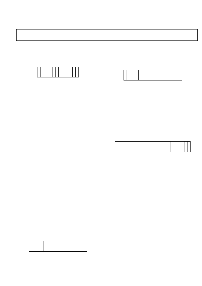
In the ADM1041, the send byte protocol is used to write a
register address to RAM for a subsequent single-byte read from
the same address or block read or write starting at that address.
This is illustrated in Figure 30.
Rev. A | Page 37 of 64
SLAVE
ADDRESS
S
RAM
ADDRESS
(00h TO 7Fh)
W A
A P
4
5
6
2
1
3
0
Figure 30. Setting a RAM Address for Subsequent Read
If it is required to read data from the RAM immediately after
setting up the address, the master can assert a repeat start
condition immediately after the final ACK and carry out a
single-byte read, block read, or block write operation without
asserting an intermediate stop condition.
Write Byte/Word
In this operation, the master device sends a command byte and
one or two data bytes to the slave device, as follows:
1.
The master device asserts a start condition on SDA.
2.
The master sends the 7-bit slave address followed by the
write bit (low).
3.
The addressed slave device asserts ACK on SDA.
4.
The master sends a command code.
5.
The slave asserts ACK on SDA.
6.
The master sends a data byte.
7.
The slave asserts ACK on SDA.
8.
The master sends a data byte (or may assert stop at this
point).
9.
The slave asserts ACK on SDA.
10.
The master asserts a stop condition on SDA to end the
transaction.
In the ADM1041, the write byte/word protocol is used for the
following three purposes. The ADM1041 knows how to respond
by the value of the command byte.
Write a single byte of data to RAM. In this case, the
command byte is the RAM address from 00h to 7Fh and
the (only) data byte is the actual data. This is illustrated in
Figure 31.
SLAVE
ADDRESS
S
DATA
W A
A P
A
6
7
8
5
2
1
3
0
RAM
ADDRESS
(00h TO 7Fh)
4
Figure 31. Single-Byte Write to RAM
Set up a 2-byte EEPROM address for a subsequent read or
block read. In this case, the command byte is the high byte
of the EEPROM address (80h). The (only) data byte is the
low byte of the EEPROM address. This is illustrated in
Figure 32.
SLAVE
ADDRESS
S
EEPROM
ADDRESS
HIGH BYTE
(80h OR 81h)
EEPROM
ADDRESS
LOW BYTE
(00h TO FFh)
W
A P
A
A
6
7
8
5
2
1
4
3
0
Figure 32. Setting an EEPROM Address
If it is required to read data from the EEPROM immedi-
ately after setting up the address, the master can assert a
repeat start condition immediately after the final ACK and
carry out a single-byte read or a block read without
asserting an intermediate stop condition.
Write a single byte of data to EEPROM. In this case, the
command byte is the high byte of the EEPROM address,
80h or 81h. The first data byte is the low byte of the
EEPROM address and the second data byte is the actual
data. Bit 1 of EEPROM Register 3 must be set. This is
illustrated in Figure 33.
SLAVE
ADDRESS
S
EEPROM
ADDRESS
HIGH BYTE
(80h OR 81h)
EEPROM
ADDRESS
LOW BYTE
(00h TO FFh)
W A
A P
A
5
A
6
9 10
7
2
1
4
3
0
DATA
8
Figure 33. Single-Byte Write to EEPROM
If it is required to read data from the ASIC immediately after
setting up the address, the master can assert a repeat start
condition immediately after the final ACK and carry out a
single-byte read, block read, or block write operation without
asserting an intermediate stop condition.
Block Write
In this operation, the master device writes a block of data to a
slave device. Programming an EEPROM byte takes approximately
300 μs, which limits the SMBus clock for repeated or block write
operations. The start address for a block write must have been
set previously. In the case of the ADM1041, this is done by a
send byte operation to set a RAM address or by a write byte/
word operation to set an EEPROM address.
1.
The master device asserts a start condition on SDA.
2.
The master sends the 7-bit slave address followed by the
write bit (low).
3.
The addressed slave device asserts ACK on SDA.
4.
The master sends a command code that tells the slave
device to expect a block write. The ADM1041 command
code for a block read is A0h (10100000).
5.
The slave asserts ACK on SDA.
相關PDF資料 |
PDF描述 |
|---|---|
| ADM1041A | Secondary-Side Controller with Current Share and Housekeeping |
| ADM1041AARQZ | Secondary-Side Controller with Current Share and Housekeeping |
| ADM1041AARQZ-REEL | Secondary-Side Controller with Current Share and Housekeeping |
| ADM1041AARQZ-REEL7 | Secondary-Side Controller with Current Share and Housekeeping |
| ADM1052 | Precision Dual Voltage Regulator Controller |
相關代理商/技術參數 |
參數描述 |
|---|---|
| ADM1041ARQ-2 | 制造商:Rochester Electronics LLC 功能描述: 制造商:Analog Devices 功能描述: |
| ADM1041ARQ-REEL | 制造商:AD 制造商全稱:Analog Devices 功能描述:Secondary-Side Controller with Current Share and Housekeeping |
| ADM1041ARQ-REEL7 | 功能描述:IC PWR SUP MON/LOAD SHARE 24QSOP RoHS:否 類別:集成電路 (IC) >> PMIC - 電源控制器,監視器 系列:- 產品培訓模塊:Lead (SnPb) Finish for COTS Obsolescence Mitigation Program 標準包裝:2,500 系列:- 應用:多相控制器 輸入電壓:- 電源電壓:9 V ~ 14 V 電流 - 電源:- 工作溫度:-40°C ~ 85°C 安裝類型:表面貼裝 封裝/外殼:40-WFQFN 裸露焊盤 供應商設備封裝:40-TQFN-EP(5x5) 包裝:帶卷 (TR) |
| ADM1041ARQZ | 功能描述:IC PWR SUPP MON/LOAD SHAR 24QSOP RoHS:是 類別:集成電路 (IC) >> PMIC - 電源控制器,監視器 系列:- 產品培訓模塊:Lead (SnPb) Finish for COTS Obsolescence Mitigation Program 標準包裝:2,500 系列:- 應用:多相控制器 輸入電壓:- 電源電壓:9 V ~ 14 V 電流 - 電源:- 工作溫度:-40°C ~ 85°C 安裝類型:表面貼裝 封裝/外殼:40-WFQFN 裸露焊盤 供應商設備封裝:40-TQFN-EP(5x5) 包裝:帶卷 (TR) |
| ADM1041ARQZ-REEL | 功能描述:IC SECONDARY SIDE CTRLR 24QSOP RoHS:是 類別:集成電路 (IC) >> PMIC - 電源控制器,監視器 系列:- 產品培訓模塊:Lead (SnPb) Finish for COTS Obsolescence Mitigation Program 標準包裝:2,500 系列:- 應用:多相控制器 輸入電壓:- 電源電壓:9 V ~ 14 V 電流 - 電源:- 工作溫度:-40°C ~ 85°C 安裝類型:表面貼裝 封裝/外殼:40-WFQFN 裸露焊盤 供應商設備封裝:40-TQFN-EP(5x5) 包裝:帶卷 (TR) |
發布緊急采購,3分鐘左右您將得到回復。