- 您現在的位置:買賣IC網 > PDF目錄373996 > ADM1064ACP-REEL7 (ANALOG DEVICES INC) Super Sequencer with Voltage Readback ADC PDF資料下載
參數資料
| 型號: | ADM1064ACP-REEL7 |
| 廠商: | ANALOG DEVICES INC |
| 元件分類: | 電源管理 |
| 英文描述: | Super Sequencer with Voltage Readback ADC |
| 中文描述: | 10-CHANNEL POWER SUPPLY SUPPORT CKT, QCC40 |
| 封裝: | 6 X 6 MM, MO-220-VJJD-2, LFCS-40 |
| 文件頁數: | 26/32頁 |
| 文件大小: | 523K |
| 代理商: | ADM1064ACP-REEL7 |
第1頁第2頁第3頁第4頁第5頁第6頁第7頁第8頁第9頁第10頁第11頁第12頁第13頁第14頁第15頁第16頁第17頁第18頁第19頁第20頁第21頁第22頁第23頁第24頁第25頁當前第26頁第27頁第28頁第29頁第30頁第31頁第32頁
ADM1064
Rev. 0 | Page 26 of 32
5
6
P
To erase a page of EEPROM memory. EEPROM memory
can be written to only if it is unprogrammed. Before
writing to one or more EEPROM memory locations that
are already programmed, the page or pages containing
those locations must first be erased. EEPROM memory is
erased by writing a command byte.
The master sends a command code that tells the slave
device to erase the page. The ADM1064 command code for
a page erasure is 0xFE (1111 1110). Note that, for a page
erasure to take place, the page address has to be given in
the previous write word transaction (see the Write
Byte/Word section). Also, Bit 2 in the UPDCFG register
(Address 0x90) must be set to 1.
0
2
4
1
3
SLAVE
ADDRESS
COMMAND
BYTE
(0xFE)
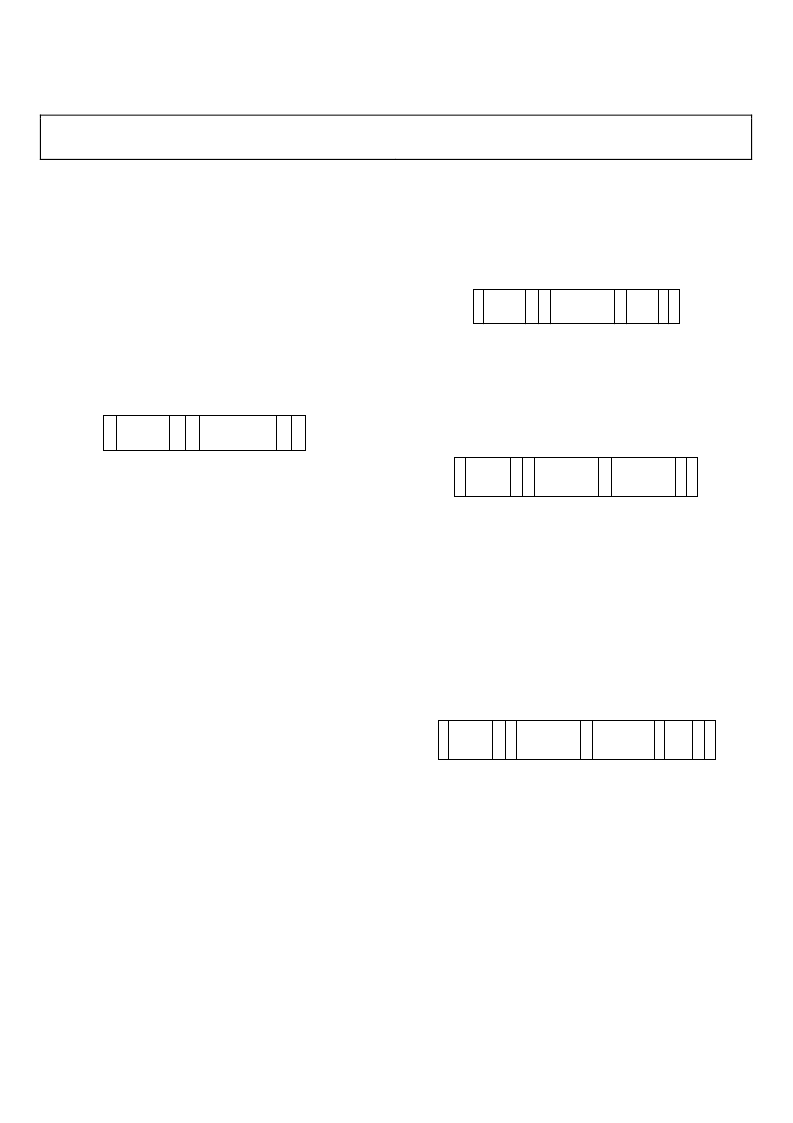
S
W
A
A
Figure 35. EEPROM Page Erasure
As soon as the ADM1064 receives the command byte, page
erasure begins. The master device can send a stop
command as soon as it sends the command byte. Page
erasure takes approximately 20 ms. If the ADM1064 is
accessed before erasure is complete, it responds with a no
acknowledge (NACK).
Write Byte/Word
In a write byte/word operation, the master device sends a
command byte and one or two data bytes to the slave device, as
follows:
1.
The master device asserts a start condition on SDA.
2.
The master sends the 7-bit slave address followed by the
write bit (low).
3.
The addressed slave device asserts ACK on SDA.
4.
The master sends a command code.
5.
The slave asserts ACK on SDA.
6.
The master sends a data byte.
7.
The slave asserts ACK on SDA.
8.
The master sends a data byte (or asserts a stop condition at
this point).
9.
The slave asserts ACK on SDA.
10.
The master asserts a stop condition on SDA to end the
transaction.
In the ADM1064, the write byte/word protocol is used for three
purposes:
To write a single byte of data to RAM. In this case, the
command byte is the RAM address from 0x00 to 0xDF and
the only data byte is the actual data, as shown in Figure 36.
0
ASLAVE
ARAM
(0x00 TO 0xDF)
S
W A
DATA
A
P
A
2
4
1
3
5
7
6
8
Figure 36. Single Byte Write to RAM
To set up a 2-byte EEPROM address for a subsequent read,
write, block read, block write, or page erase. In this case, the
command byte is the high byte of the EEPROM address
from 0xF8 to 0xFB. The only data byte is the low byte of
the EEPROM address, as shown in Figure 37.
0
SLAVE
ADDRESS
EEPROM
ADDRESS
HIGH BYTE
(0xF8 TO 0xFB)
S
W A
EEPROM
ADDRESS
LOW BYTE
(0x00 TO 0xFF)
A
P
A
2
4
1
3
5
7
6
8
Figure 37. Setting an EEPROM Address
Note, for page erasure, that because a page consists of
32 bytes, only the three MSBs of the address low byte are
important. The lower five bits of the EEPROM address low
byte specify the addresses within a page and are ignored
during an erase operation.
To write a single byte of data to EEPROM. In this case, the
command byte is the high byte of the EEPROM address
from 0xF8 to 0xFB. The first data byte is the low byte of the
EEPROM address, and the second data byte is the actual
data, as shown in Figure 38.
0
SLAVE
ADDRESS
EEPROM
ADDRESS
HIGH BYTE
(0xF8 TO 0xFB)
S
W A
EEPROM
ADDRESS
LOW BYTE
(0x00 TO 0xFF)
A
P
A
2
4
1
3
5
7
A
9
DATA
8
6
10
Figure 38. Single Byte Write to EEPROM
Block Write
In a block write operation, the master device writes a block of
data to a slave device. The start address for a block write must
have been set previously. In the ADM1064, a send byte opera-
tion sets a RAM address, and a write byte/word operation sets
an EEPROM address, as follows:
1.
The master device asserts a start condition on SDA.
2.
The master sends the 7-bit slave address followed by
the write bit (low).
3.
The addressed slave device asserts ACK on SDA.
4.
The master sends a command code that tells the slave
device to expect a block write. The ADM1064 command
code for a block write is 0xFC (1111 1100).
相關PDF資料 |
PDF描述 |
|---|---|
| ADM1064ASU | Super Sequencer with Voltage Readback ADC |
| ADM1064ASU-REEL | Super Sequencer with Voltage Readback ADC |
| ADM1064ASU-REEL7 | Super Sequencer with Voltage Readback ADC |
| ADM1065 | Super Sequencer-TM and Monitor |
| ADM1065ACP | Super Sequencer-TM and Monitor |
相關代理商/技術參數 |
參數描述 |
|---|---|
| ADM1064ACPZ | 功能描述:IC SEQUENCER/SUPERVISOR 40-LFCSP RoHS:是 類別:集成電路 (IC) >> PMIC - 監控器 系列:Super Sequencer® 標準包裝:1 系列:- 類型:簡單復位/加電復位 監視電壓數目:1 輸出:開路漏極或開路集電極 復位:高有效 復位超時:- 電壓 - 閥值:1.8V 工作溫度:-40°C ~ 125°C 安裝類型:表面貼裝 封裝/外殼:6-TSOP(0.059",1.50mm 寬)5 引線 供應商設備封裝:5-TSOP 包裝:剪切帶 (CT) 其它名稱:NCP301HSN18T1GOSCT |
| ADM1064ASU | 制造商:Analog Devices 功能描述:Volt Supervisor Sequencer 2.7V to 5.4V 48-Pin TQFP |
| ADM1064ASU-REEL | 制造商:Analog Devices 功能描述:Volt Supervisor Sequencer 2.7V to 5.4V 48-Pin TQFP T/R |
| ADM1064ASU-REEL7 | 制造商:Analog Devices 功能描述:Volt Supervisor Sequencer 2.7V to 5.4V 48-Pin TQFP T/R |
| ADM1064ASUZ | 功能描述:IC SEQUENCER/SUPERVISOR 48-TQFP RoHS:是 類別:集成電路 (IC) >> PMIC - 監控器 系列:Super Sequencer® 其它有關文件:STM6905 View All Specifications 標準包裝:1 系列:- 類型:多壓監控器 監視電壓數目:5 輸出:開路漏極或開路集電極 復位:低有效 復位超時:最小為 140 ms 電壓 - 閥值:2.188V,2.955V,可調,可調,可調 工作溫度:-40°C ~ 85°C 安裝類型:表面貼裝 封裝/外殼:8-TSSOP,8-MSOP(0.118",3.00mm 寬) 供應商設備封裝:8-TSSOP 包裝:Digi-Reel® 產品目錄頁面:1197 (CN2011-ZH PDF) 其它名稱:497-8728-6 |
發布緊急采購,3分鐘左右您將得到回復。