- 您現在的位置:買賣IC網 > PDF目錄373996 > ADM1065ASU-REEL (ANALOG DEVICES INC) Super Sequencer-TM and Monitor PDF資料下載
參數資料
| 型號: | ADM1065ASU-REEL |
| 廠商: | ANALOG DEVICES INC |
| 元件分類: | 電源管理 |
| 英文描述: | Super Sequencer-TM and Monitor |
| 中文描述: | 10-CHANNEL POWER SUPPLY SUPPORT CKT, PQFP48 |
| 封裝: | 7 X 7 MM, PLASTIC, MS-026ABC, TQFP-48 |
| 文件頁數: | 17/28頁 |
| 文件大小: | 497K |
| 代理商: | ADM1065ASU-REEL |
第1頁第2頁第3頁第4頁第5頁第6頁第7頁第8頁第9頁第10頁第11頁第12頁第13頁第14頁第15頁第16頁當前第17頁第18頁第19頁第20頁第21頁第22頁第23頁第24頁第25頁第26頁第27頁第28頁
ADM1065
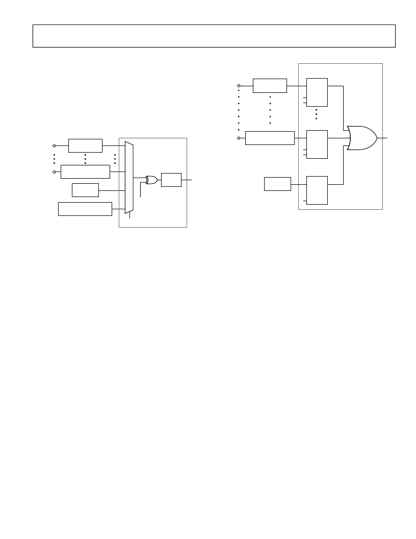
SEQUENCE DETECTOR
The sequence detector block is used to detect when a step in a
sequence has been completed. It looks for one of the inputs to
the SE to change state, and is most often used as the gate on
successful progress through a power-up or power-down
sequence. A timer block is included in this detector, which can
insert delays into a power-up or power-down sequence, if
required. Timer delays can be set from 10 μs to 400 ms.
Figure 22 is a block diagram of the sequence detector.
Rev. 0 | Page 17 of 28
0
SUPPLY FAULT
DETECTION
LOGIC INPUT CHANGE
OR FAULT DETECTION
WARNINGS
FORCE FLOW
(UNCONDITIONAL JUMP)
VP1
VX5
INVERT
SEQUENCE
DETECTOR
SELECT
TIMER
Figure 22. Sequence Detector Block Diagram
The sequence detector can also help to identify monitoring
faults. In the sample application shown in Figure 21, the FSEL1
and FSEL2 states first identify which of the VP1,VP2, or VP3
pins has faulted, and then they take the appropriate action.
MONITORING FAULT DETECTOR
The monitoring fault detector block is used to detect a failure
on an input. The logical function implementing this is a wide
OR gate, which can detect when an input deviates from its
expected condition. The clearest demonstration of the use of
this block is in the PWRGD state, where the monitor block
indicates that a failure on one or more of the VP1,VP2, or VP3
inputs has occurred.
No programmable delay is available in this block, because the
triggering of a fault condition is likely to be caused when a
supply falls out of tolerance. In this situation, the user would
want to react as quickly as possible. Some latency occurs when
moving out of this state, however, because it takes a finite
amount of time (~20 μs) for the state configuration to
download from EEPROM into the SE. Figure 23 is a block
diagram of the monitoring fault detector.
0
SUPPLY FAULT
DETECTION
LOGIC INPUT CHANGE
OR FAULT DETECTION
VP1
VX5
MONITORING FAULT
DETECTOR
MASK
SENSE
1-BIT FAULT
DETECTOR
FAULT
WARNINGS
MASK
1-BIT FAULT
DETECTOR
FAULT
MASK
SENSE
1-BIT FAULT
DETECTOR
FAULT
Figure 23. Monitoring Fault Detector Block Diagram
TIMEOUT DETECTOR
The timeout detector allows the user to trap a failure to make
proper progress through a power-up or power-down sequence.
In the sample application shown in Figure 21, the timeout next-
state transition is from the EN3V3 and EN2V5 states. For the
EN3V3 state, the signal 3V3ON is asserted upon entry to this
state (on the PDO1 output pin) to turn on a 3.3 V supply. This
supply rail is connected to the VP2 pin, and the sequence detec-
tor looks for the VP2 pin to go above its UV threshold, which is
set in the supply fault detector (SFD) attached to that pin.
The power-up sequence progresses when this change is
detected. If, however, the supply fails (perhaps due to a short
circuit overloading this supply), then the timeout block traps
the problem. In this example, if the 3.3 V supply fails within
10 ms, then the SE moves to the DIS3V3 state and turns off this
supply by bringing PDO1 low. It also indicates that a fault has
occurred by taking PDO3 high. Timeout delays of from 100 μs
to 400 ms can be programmed.
FAULT REPORTING
The ADM1065 has a fault latch for recording faults. Two
registers are set aside for this purpose. A single bit is assigned to
each input of the device, and a fault on that input sets the
relevant bit. The contents of the fault register can be read out
over the SMBus to determine which input(s) faulted. The fault
register can be enabled/disabled in each state. This ensures that
only real faults are captured and not, for example, undervoltage
trips when the SE is executing a power-down sequence.
相關PDF資料 |
PDF描述 |
|---|---|
| ADM1065ASU-REEL7 | Super Sequencer-TM and Monitor |
| ADM1066ASU-REEL | Multisupply Supervisor/Sequencer with Margining Control and Auxiliary ADC Inputs |
| ADM1066ASU-REEL7 | Multisupply Supervisor/Sequencer with Margining Control and Auxiliary ADC Inputs |
| ADM1066ASU-U3 | Multisupply Supervisor/Sequencer with Margining Control and Auxiliary ADC Inputs |
| ADM1066ACP | Multisupply Supervisor/Sequencer with Margining Control and Auxiliary ADC Inputs |
相關代理商/技術參數 |
參數描述 |
|---|---|
| ADM1065ASU-REEL7 | 制造商:AD 制造商全稱:Analog Devices 功能描述:Super Sequencer-TM and Monitor |
| ADM1065ASUZ | 功能描述:IC SEQUENCER/MONITOR 48-TQFP RoHS:是 類別:集成電路 (IC) >> PMIC - 監控器 系列:Super Sequencer® 標準包裝:1 系列:- 類型:簡單復位/加電復位 監視電壓數目:1 輸出:開路漏極或開路集電極 復位:高有效 復位超時:- 電壓 - 閥值:1.8V 工作溫度:-40°C ~ 125°C 安裝類型:表面貼裝 封裝/外殼:6-TSOP(0.059",1.50mm 寬)5 引線 供應商設備封裝:5-TSOP 包裝:剪切帶 (CT) 其它名稱:NCP301HSN18T1GOSCT |
| ADM1065ASUZ-RL7 | 功能描述:IC SEQUENCER/MONITOR 48-TQFP 制造商:analog devices inc. 系列:Super Sequencer? 包裝:剪切帶(CT) 零件狀態:在售 類型:序列發生器 受監控電壓數:10 輸出:可編程 復位:- 復位超時:- 電壓 - 閾值:可調節/可選擇 工作溫度:-40°C ~ 85°C(TA) 安裝類型:表面貼裝 封裝/外殼:48-TQFP 供應商器件封裝:48-TQFP(7x7) 標準包裝:1 |
| ADM1066 | 制造商:AD 制造商全稱:Analog Devices 功能描述:Multisupply Supervisor/Sequencer with Margining Control and Auxiliary ADC Inputs |
| ADM1066ACP | 制造商:Analog Devices 功能描述:Volt Supervisor Sequencer 2.7V to 5.4V 40-Pin LFCSP EP 制造商:Analog Devices 功能描述:IC SEQUENCER/SUPERVISOR |
發布緊急采購,3分鐘左右您將得到回復。