- 您現(xiàn)在的位置:買賣IC網(wǎng) > PDF目錄373999 > ADM203 (Analog Devices, Inc.) Low Power 5V RS232 Dual Driver/Receiver with 0.1?μF Capacitors; Package: SO; No of Pins: 16; Temperature Range: -40?°C to 85?°C PDF資料下載
參數(shù)資料
| 型號: | ADM203 |
| 廠商: | Analog Devices, Inc. |
| 元件分類: | 外設(shè)及接口 |
| 英文描述: | Low Power 5V RS232 Dual Driver/Receiver with 0.1?μF Capacitors; Package: SO; No of Pins: 16; Temperature Range: -40?°C to 85?°C |
| 中文描述: | 電可擦除可編程邏輯器件 |
| 文件頁數(shù): | 4/6頁 |
| 文件大小: | 305K |
| 代理商: | ADM203 |
ADM202/ADM203
REV. 0
–4–
R
IN
Receiver Inputs. These inputs accept RS-232 signal levels. An internal 5 k
pull-down resistor to GND is
connected on each of these inputs.
Receiver Outputs. These are TTL/CMOS levels.
R
OUT
GENERAL INFORMATION
The ADM202/ADM203 is an RS-232 drivers/receivers designed
to solve interface problems by meeting the EIA-232E specifica-
tions while using a single digital +5 V supply. The EIA standard
requires transmitters that will deliver
±
5 V minimum on the
transmission channel and receivers that can accept signal levels
down to
±
3 V. The parts achieve this by integrating step up
voltage converters and level shifting transmitters and receivers
onto the same chip. CMOS technology is used to keep the
power dissipation to an absolute minimum.
The ADM203 uses internal capacitors and, therefore, no exter-
nal capacitors are required.
The ADM202 contains an internal voltage doubler and a voltage
inverter which generates
±
10 V from the +5 V input. External
0.1
μ
F capacitors are required for the internal voltage converter.
The ADM202/ADM203 is a modification, enhancement and
improvement to the AD230–AD241 family and derivatives
thereof. It is essentially plug-in compatible and does not have
materially different applications.
CIRCUIT DESCRIPTION
The internal circuitry consists of three main sections. These are
(a) A Charge Pump Voltage Converter
(b) RS-232 to TTL/CMOS Receivers
(c) TTL/CMOS to RS-232 Transmitters
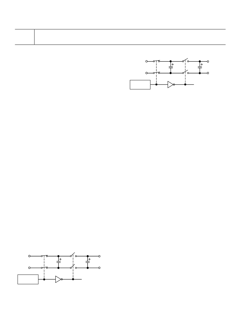
Charge Pump DC-DC Voltage Converter
The charge pump voltage converter consists of an oscillator and
a switching matrix. The converter generates a
±
10 V supply
from the input 5 V level. This is done in two stages using a
switched capacitor technique as illustrated below. First, the 5 V
input supply is doubled to 10 V using capacitor C1 as the
charge storage element. The 10 V level is then inverted to gen-
erate –10 V using C2 as the storage element.
Capacitors C3 and C4 are used to reduce the output ripple.
Their values are not critical and can be reduced if higher levels
of ripple are acceptable. The charge pump capacitors C1 and
C2 may also be reduced at the expense of higher output imped-
ance on the V+ and V– supplies. On the ADM203, all capaci-
tors C1 to C4 are molded into the package.
The V+ and V– supplies may also be used to power external
circuitry if the current requirements are small.
S1
S3
V+ = 2V
CC
S2
S4
INTERNAL
OSCILLATOR
C1
C3
V
CC
GND
V
CC
Figure 2. Charge Pump Voltage Doubler
S1
S3
S2
S4
INTERNAL
OSCILLATOR
C2
C4
V– = – (V+)
GND
V+
GND
FROM
VOLTAGE
DOUBLER
Figure 3. Charge Pump Voltage Inverter
Transmitter (Driver) Section
The drivers convert TTL/CMOS input levels into EIA-232-E
output levels. With V
CC
= +5 V and driving a typical EIA-232-E
load, the output voltage swing is
±
9 V. Even under worst case
conditions the drivers are guaranteed to meet the
±
5 V
EIA-232-E minimum requirement.
The input threshold levels are both TTL and CMOS compat-
ible with the switching threshold set at V
CC
/4. With a nominal
V
CC
= 5 V the switching threshold is 1.25 V typical. Unused
inputs may be left unconnected, as an internal 400 k
pull-up
resistor pulls them high forcing the outputs into a low state.
As required by the EIA-232-E standard the slew rate is limited
to less than 30 V/
μ
s without the need for an external slew limiting
capacitor and the output impedance in the power-off state is
greater than 300
.
Receiver Section
The receivers are inverting level shifters that accept EIA-232-E
input levels (
±
5 V to
±
15 V) and translate them into 5 V TTL/
CMOS levels. The inputs have internal 5 k
pull-down resistors
to ground and are also protected against overvoltages of up to
±
30 V. The guaranteed switching thresholds are 0.8 V minimum
and 2.4 V maximum which are well within the
±
3 V EIA-232
requirement. The low level threshold is deliberately positive as it
ensures that an unconnected input will be interpreted as a low
level.
The receivers have Schmitt trigger input with a hysteresis level
of 0.5 V. This ensures error free reception both for noisy inputs
and for inputs with slow transition times.
相關(guān)PDF資料 |
PDF描述 |
|---|---|
| ADM202JRW | Low Power 5V RS232 Dual Driver/Receiver with 0.1?μF Capacitors; Package: SO; No of Pins: 16; Temperature Range: -40?°C to 85?°C |
| ADM202JN | Low Power 5V RS232 Dual Driver/Receiver with 0.1?μF Capacitors; Package: SO; No of Pins: 16; Temperature Range: -40?°C to 85?°C |
| ADM202 | Low Power 5V RS232 Dual Driver/Receiver with 0.1?μF Capacitors; Package: SO; No of Pins: 16; Temperature Range: -40?°C to 85?°C |
| ADM202JRN | Aluminum Electrolytic Radial Leaded Bi-Polar Capacitor; Capacitance: 47uF; Voltage: 100V; Case Size: 12.5x20 mm; Packaging: Bulk |
| ADM203JN | Low Power 5V RS232 Dual Driver/Receiver with 0.1?μF Capacitors; Package: SO; No of Pins: 16; Temperature Range: -40?°C to 85?°C |
相關(guān)代理商/技術(shù)參數(shù) |
參數(shù)描述 |
|---|---|
| ADM203JN | 制造商:Analog Devices 功能描述:Dual Transmitter/Receiver RS-232 20-Pin PDIP N 制造商:Analog Devices 功能描述:LINE TRANSMITTER/RCVR 2TR 2TX 2RX 20PDIP N - Rail/Tube 制造商:Analog Devices 功能描述:IC TRANSCEIVER RS232 |
| ADM203JNZ | 制造商:Analog Devices 功能描述:Dual Transmitter/Receiver RS-232 20-Pin PDIP N 制造商:Analog Devices 功能描述:LINE TRANSMITTER/RCVR 2TR 2TX 2RX 20PDIP - Rail/Tube 制造商:Rochester Electronics LLC 功能描述:0.1UF LINE DRIVER - Bulk |
| ADM205 | 制造商:AD 制造商全稱:Analog Devices 功能描述:0.1 uF, +5 V Powered CMOS RS-232 Drivers/Receivers |
| ADM205-ADM211 | 制造商:AD 制造商全稱:Analog Devices 功能描述:0.1 mF. +5 V Powered CMOS RS-232 Drivers/Receivers |
| ADM205AN | 制造商:AD 制造商全稱:Analog Devices 功能描述:0.1 uF, +5 V Powered CMOS RS-232 Drivers/Receivers |
發(fā)布緊急采購,3分鐘左右您將得到回復(fù)。