- 您現在的位置:買賣IC網 > PDF目錄374003 > ADM3307E (Analog Devices, Inc.) 15 kV ESD Protected, 2.7 V to 3.6 V Serial Port Transceivers with Green Idle⑩ PDF資料下載
參數資料
| 型號: | ADM3307E |
| 廠商: | Analog Devices, Inc. |
| 英文描述: | 15 kV ESD Protected, 2.7 V to 3.6 V Serial Port Transceivers with Green Idle⑩ |
| 中文描述: | 15 kV的ESD保護,2.7 V到3.6 V綠色串口收發器閑置⑩ |
| 文件頁數: | 11/16頁 |
| 文件大小: | 312K |
| 代理商: | ADM3307E |
REV. G
ADM3307E/ADM3310E/ADM3311E/ADM3312E/ADM3315E
–11–
CIRCUIT DESCRIPTION
The internal circuitry consists mainly of four sections. These
include the following:
1. A charge pump voltage converter
2. 3.3 V logic to EIA-232 transmitters
3. EIA-232 to 3.3 V logic receivers
4. Transient protection circuit on all I/O lines
Charge Pump DC-to-DC Voltage Converter
The charge pump voltage converter consists of a 250 kHz (300 kHz
for ADM3307E) oscillator and a switching matrix. The converter
generates a
±
9 V supply from the input 3.0 V level. This is done
in two stages using a switched capacitor technique, as illustrated.
First, the 3.0 V input supply is tripled to 9.0 V using capacitor
C4 as the charge storage element. The +9.0 V level is then
inverted to generate
–
9.0 V using C5 as the storage element.
However, it should be noted that, unlike other charge pump dc-to-
dc converters, the charge pump on the ADM3307E does not run
open-loop. The output voltage is regulated to
±
7.25 V (or
±
6.5 V
for the ADM3310E and ADM3315E) by the Green Idle circuit
and never reaches
±
9 V in practice. This saves power as well as
maintains a more constant output voltage.
+
+
INTERNAL
OSCILLATOR
GND
C2
C1
S1
S2
S3
S4
V
CC
+
C4
V+ = 3V
CC
V
CC
V
CC
S5
S6
S7
Figure 1. Charge Pump Voltage Tripler
The tripler operates in two phases. During the oscillator low
phase, S1 and S2 are closed and C1 charges rapidly to V
CC
.
S3, S4, and S5 are open, and S6 and S7 are closed.
During the oscillator high phase, S1 and S2 are open, and S3
and S4 are closed, so the voltage at the output of S3 is 2V
CC
.
This voltage is used to charge C2. In the absence of any dis-
charge current, C2 charges up to 2V
CC
after several cycles.
During the oscillator high phase, as previously mentioned, S6
and S7 are closed, so the voltage at the output of S6 is 3V
CC
.
This voltage is then used to charge C3. The voltage inverter
is illustrated in Figure 2.
FROM
VOLTAGE
TRIPLER
+
+
INTERNAL
OSCILLATOR
GND
C5
C3
S8
S9
S10
S11
V+
GND
V– = –(V+)
Figure 2. Charge Pump Voltage Inverter
During the oscillator high phase, S10 and S11 are open, while
S8 and S9 are closed. C3 is charged to 3V
CC
from the output of
the voltage tripler over several cycles. During the oscillator low
phase, S8 and S9 are open, while S10 and S11 are closed. C3 is
connected across C5, whose positive terminal is grounded and
whose negative terminal is the V
–
output. Over several cycles,
C5 charges to
–
3 V
CC
.
The V+ and V
–
supplies may also be used to power external
circuitry if the current requirements are small. Please refer to
TPC 3 in the Typical Performance Characteristics section.
What Is Green Idle
Green Idle is a method of minimizing power consumption under
idle (no transmit) conditions while still maintaining the ability to
transmit data instantly.
How Does it Work
Charge pump type dc-to-dc converters used in RS-232 line drivers
normally operate open-loop, i.e., the output voltage is not regu-
lated in any way. Under light load conditions, the output voltage
is close to twice the supply voltage for a doubler and three times
the supply voltage for a tripler, with very little ripple. As the load
current increases, the output voltage falls and the ripple voltage
increases.
Even under no-load conditions, the oscillator and charge pump
operate at a very high frequency with consequent switching losses
and current drain.
Green Idle works by monitoring the output voltage and maintain-
ing it at a constant value of around 7 V
*
. When the voltage rises
above 7.25 V
**
the oscillator is turned off. When the voltage falls
below 7 V
*
, the oscillator is turned on and a burst of charging
pulses is sent to the reservoir capacitor. When the oscillator is
turned off, the power consumption of the charge pump is virtu-
ally zero, so the average current drain under light load conditions
is greatly reduced.
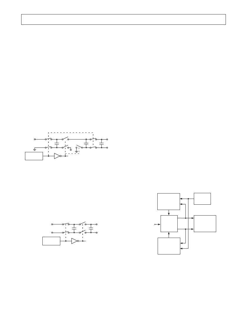
A block diagram of the Green Idle circuit is shown in Figure 3.
Both V+ and V
–
are monitored and compared to a reference
voltage derived from an on-chip band gap device. If either V+
or V
–
fall below 7 V
*
, the oscillator starts up until the
voltage rises above 7.25
V
**
.
V– VOLTAGE
COMPARATOR
WITH 250mV
HYSTERESIS
BAND GAP
VOLTAGE
REFERENCE
V+ VOLTAGE
COMPARATOR
WITH 250mV
HYSTERESIS
TRANSCEIVERS
CHARGE
PUMP
START/STOP
START/STOP
V+
V–
SHUTDOWN
Figure 3. Block Diagram of Green Idle Circuit
NOTES
*
For ADM3310E and ADM3315E, replace with 6.25 V.
**
For ADM3310E and ADM3315E, replace with 6.5 V.
相關PDF資料 |
PDF描述 |
|---|---|
| ADM3312E | 15 kV ESD Protected, 2.7 V to 3.6 V Serial Port Transceivers with Green Idle⑩ |
| ADM3315 | 15 kV ESD Protected, 2.7 V to 3.6 V Serial Port Transceivers with Green Idle⑩ |
| ADM3310EACP | 15 kV ESD Protected, 2.7 V to 3.6 V Serial Port Transceivers with Green Idle⑩ |
| ADM3312EACP | 15 kV ESD Protected, 2.7 V to 3.6 V Serial Port Transceivers with Green Idle⑩ |
| ADM3310EACP-REEL | 15 kV ESD Protected, 2.7 V to 3.6 V Serial Port Transceivers with Green Idle⑩ |
相關代理商/技術參數 |
參數描述 |
|---|---|
| ADM3307EACP | 制造商:Analog Devices 功能描述:Quint Transmitter Triple Receiver RS-232 32-Pin LFCSP EP 制造商:Rochester Electronics LLC 功能描述:15KV ESD, +2.7V TO 3.6V SERIAL PORT I.C. - Bulk |
| ADM3307EACP-REEL | 制造商:Analog Devices 功能描述:Quint Transmitter Triple Receiver RS-232 32-Pin LFCSP EP T/R 制造商:Analog Devices 功能描述:LINE TRANSMITTER/RCVR 3TR 5TX 3RX 32LFCSP EP - Tape and Reel |
| ADM3307EACP-REEL7 | 制造商:Analog Devices 功能描述:Quint Transmitter Triple Receiver RS-232 32-Pin LFCSP EP T/R 制造商:Rochester Electronics LLC 功能描述:15KV ESD, +2.7V TO 3.6V SERIAL PORT I.C. - Tape and Reel |
| ADM3307EACPZ | 功能描述:IC TXRX RS-232 5:3 2.7V 32LFCSP RoHS:是 類別:集成電路 (IC) >> 接口 - 驅動器,接收器,收發器 系列:- 產品培訓模塊:RS-232 & USB Transceiver 標準包裝:2,000 系列:- 類型:收發器 驅動器/接收器數:1/1 規程:RS232 電源電壓:3 V ~ 5.5 V 安裝類型:表面貼裝 封裝/外殼:16-SSOP(0.209",5.30mm 寬) 供應商設備封裝:16-SSOP 包裝:帶卷 (TR) 其它名稱:296-19849-2 |
| ADM3307EACPZ-REEL | 功能描述:IC TXRX RS-232 5:3 2.7V 32LFCSP RoHS:是 類別:集成電路 (IC) >> 接口 - 驅動器,接收器,收發器 系列:- 標準包裝:121 系列:- 類型:收發器 驅動器/接收器數:1/1 規程:RS422,RS485 電源電壓:3 V ~ 3.6 V 安裝類型:表面貼裝 封裝/外殼:10-WFDFN 裸露焊盤 供應商設備封裝:10-DFN(3x3) 包裝:管件 |
發布緊急采購,3分鐘左右您將得到回復。