- 您現在的位置:買賣IC網 > PDF目錄374003 > ADM3307EARU (ANALOG DEVICES INC) 15 kV ESD Protected, 2.7 V to 3.6 V Serial Port Transceivers with Green Idle⑩ PDF資料下載
參數資料
| 型號: | ADM3307EARU |
| 廠商: | ANALOG DEVICES INC |
| 元件分類: | 通用總線功能 |
| 英文描述: | 15 kV ESD Protected, 2.7 V to 3.6 V Serial Port Transceivers with Green Idle⑩ |
| 中文描述: | TRIPLE LINE TRANSCEIVER, PDSO28 |
| 封裝: | MO-153AE, TSSOP-28 |
| 文件頁數: | 13/16頁 |
| 文件大小: | 312K |
| 代理商: | ADM3307EARU |
REV. G
ADM3307E/ADM3310E/ADM3311E/ADM3312E/ADM3315E
–13–
RECEIVER
OUTPUT
V
OL
EN
INPUT
t
DR
V
OH
– 0.1V
V
OL
+ 0.1V
V
OH
0V
3V
Figure 5. Receiver Disable Timing
RECEIVER
OUTPUT
EN
INPUT
t
ER
3V
0.4V
V
OH
V
OL
0V
3V
Figure 6. Receiver Enable Timing
High Baud Rate
The ADM33xxE features high slew rates, permitting data trans-
mission at rates well in excess of the EIA/RS-232E specifications.
RS-232 voltage levels are maintained at data rates up to 230 kbps
(460 kbps for ADM3307E) under worst-case loading conditions.
This allows for high speed data links between two terminals.
LAYOUT AND SUPPLY DECOUPLING
Because of the high frequencies at which the ADM33xxE oscillator
operates, particular care should be taken with printed circuit
board layout, with all traces being as short as possible and C1 to
C3 being connected as close to the device as possible. The use
of a ground plane under and around the device is also highly
recommended.
When the oscillator starts up during Green Idle operation, large
current pulses are taken from V
CC
. For this reason, V
CC
should be
decoupled with a parallel combination of 10
m
F tantalum and
0.1
m
F ceramic capacitors, mounted as close to the V
CC
pin as
possible.
Capacitors C1 to C3 can have values between 0.1
m
F and 1
m
F.
Larger values give lower ripple. These capacitors can be either
electrolytic capacitors chosen for low equivalent series resistance
(ESR) or nonpolarized types, but the use of ceramic types is
highly recommended. If polarized electrolytic capacitors are
used, polarity must be observed (as shown by C1+).
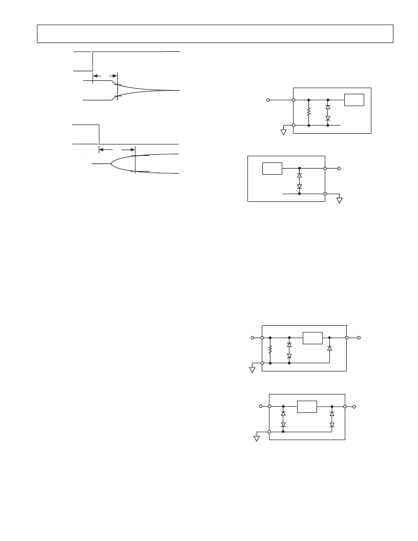
ESD/EFT TRANSIENT PROTECTION SCHEME
The ADM33xxE uses protective clamping structures on all inputs
and outputs that clamp the voltage to a safe level and dissipate
the energy present in ESD (electrostatic) and EFT (electrical fast
transients) discharges. A simplified schematic of the protection
structure is shown below in Figures 7a and 7b (see Figures 8a and
8b for ADM3307E protection structure). Each input and output
contains two back-to-back high speed clamping diodes. During nor-
mal operation with maximum RS-232 signal levels, the diodes have
no effect as one or the other is reverse biased depending on the
polarity of the signal. If however the voltage exceeds about
±
50 V,
reverse breakdown occurs and the voltage is clamped at this level.
The diodes are large p-n junctions designed to handle the
instantaneous current surge that can exceed several amperes.
The transmitter outputs and receiver inputs have a similar protec-
tion structure. The receiver inputs can also dissipate some of the
energy through the internal 5 k
W
(or 22 k
W
for the ADM3310E)
resistor to GND as well as through the protection diodes.
R
IN
Rx
D1
D2
RECEIVER
INPUT
Figure 7a. Receiver Input Protection Scheme
Tx
D1
D2
TRANSMITTER
OUTPUT
Figure 7b. Transmitter Output Protection Scheme
The ADM3307E protection scheme is slightly different (see
Figures 8a and 8b). The receiver inputs, transmitter inputs, and
transmitter outputs contain two back-to-back high speed clamping
diodes. The receiver outputs (CMOS outputs), SD and
EN
pins
contain a single reverse biased high speed clamping diode. Under
normal operation with maximum CMOS signal levels, the receiver
output, SD, and
EN
protection diodes have no effect because
they are reversed biased. If, however, the voltage exceeds about
15 V, reverse breakdown occurs and the voltage is clamped at
this level. If the voltage reaches
–
0.7 V, the diode is forward
biased and the voltage is clamped at this level. The receiver inputs
can also dissipate some of the energy through the internal 5 k
W
resistor to GND as well as through the protection diodes.
D3
R
IN
D1
D2
RECEIVER
INPUT
RECEIVER
OUTPUT
Rx
Figure 8a. ADM3307E Receiver Input Protection Scheme
Tx
D1
D2
TRANSMITTER
INPUT
TRANSMITTER
OUTPUT
D3
D4
Figure 8b. ADM3307E Transmitter Output Protection Scheme
The protection structures achieve ESD protection up to
±
15 kV on
all RS-232 I/O lines (and all CMOS lines, including SD and
EN
for the ADM3307E). The methods used to test the protection
scheme are discussed later.
相關PDF資料 |
PDF描述 |
|---|---|
| ADM3310EARU | 15 kV ESD Protected, 2.7 V to 3.6 V Serial Port Transceivers with Green Idle⑩ |
| ADM3312EARU | 15 kV ESD Protected, 2.7 V to 3.6 V Serial Port Transceivers with Green Idle⑩ |
| ADM3312EARU-REEL | 15 kV ESD Protected, 2.7 V to 3.6 V Serial Port Transceivers with Green Idle⑩ |
| ADM3307EARU-REEL7 | 15 kV ESD Protected, 2.7 V to 3.6 V Serial Port Transceivers with Green Idle⑩ |
| ADM3312EARU-REEL7 | 15 kV ESD Protected, 2.7 V to 3.6 V Serial Port Transceivers with Green Idle⑩ |
相關代理商/技術參數 |
參數描述 |
|---|---|
| ADM3307EARU-REEL | 制造商:Analog Devices 功能描述:Quint Transmitter Triple Receiver RS-232 28-Pin TSSOP T/R |
| ADM3307EARU-REEL7 | 功能描述:IC TXRX RS-232 5:3 2.7V 28TSSOP RoHS:否 類別:集成電路 (IC) >> 接口 - 驅動器,接收器,收發器 系列:- 標準包裝:121 系列:- 類型:收發器 驅動器/接收器數:1/1 規程:RS422,RS485 電源電壓:3 V ~ 3.6 V 安裝類型:表面貼裝 封裝/外殼:10-WFDFN 裸露焊盤 供應商設備封裝:10-DFN(3x3) 包裝:管件 |
| ADM3307EARUZ | 功能描述:IC TXRX RS-232 5:3 2.7V 28TSSOP RoHS:是 類別:集成電路 (IC) >> 接口 - 驅動器,接收器,收發器 系列:- 產品培訓模塊:RS-232 & USB Transceiver 標準包裝:2,000 系列:- 類型:收發器 驅動器/接收器數:1/1 規程:RS232 電源電壓:3 V ~ 5.5 V 安裝類型:表面貼裝 封裝/外殼:16-SSOP(0.209",5.30mm 寬) 供應商設備封裝:16-SSOP 包裝:帶卷 (TR) 其它名稱:296-19849-2 |
| ADM3307EARUZ-REEL | 功能描述:IC TXRX RS-232 5:3 2.7V 28TSSOP RoHS:是 類別:集成電路 (IC) >> 接口 - 驅動器,接收器,收發器 系列:- 標準包裝:121 系列:- 類型:收發器 驅動器/接收器數:1/1 規程:RS422,RS485 電源電壓:3 V ~ 3.6 V 安裝類型:表面貼裝 封裝/外殼:10-WFDFN 裸露焊盤 供應商設備封裝:10-DFN(3x3) 包裝:管件 |
| ADM3307EARUZ-REEL7 | 功能描述:IC TXRX RS-232 5:3 2.7V 28TSSOP RoHS:是 類別:集成電路 (IC) >> 接口 - 驅動器,接收器,收發器 系列:- 標準包裝:121 系列:- 類型:收發器 驅動器/接收器數:1/1 規程:RS422,RS485 電源電壓:3 V ~ 3.6 V 安裝類型:表面貼裝 封裝/外殼:10-WFDFN 裸露焊盤 供應商設備封裝:10-DFN(3x3) 包裝:管件 |
發布緊急采購,3分鐘左右您將得到回復。