- 您現在的位置:買賣IC網 > PDF目錄374002 > ADM3311EARS (ANALOG DEVICES INC) 15 kV ESD Protected, 2.7 V to 3.6 V Serial Port Transceivers with Green Idle⑩ PDF資料下載
參數資料
| 型號: | ADM3311EARS |
| 廠商: | ANALOG DEVICES INC |
| 元件分類: | 通用總線功能 |
| 英文描述: | 15 kV ESD Protected, 2.7 V to 3.6 V Serial Port Transceivers with Green Idle⑩ |
| 中文描述: | TRIPLE LINE TRANSCEIVER, PDSO28 |
| 封裝: | MO-150AH, SSOP-28 |
| 文件頁數: | 6/12頁 |
| 文件大小: | 180K |
| 代理商: | ADM3311EARS |
ADM3311E
–6–
REV. A
GENERAL DESCRIPTION
The ADM3311E is a ruggedized RS-232 line driver/receiver
that operates from a single supply of +2.7 V to +3.6 V. Step-up
voltage converters, coupled with level-shifting transmitters and
receivers, allow RS-232 levels to be developed while operating
from a single supply. Features include low power consumption,
Green Idle
operation, high transmission rates and compatibility
with the EU directive on electromagnetic compatibility. EM
compatibility includes protection against radiated and conducted
interference including high levels of electrostatic discharge.
All RS-232 inputs and outputs contain protection against
electrostatic discharges up to
±
15 kV and electrical fast tran-
sients up to
±
4 kV.
The device is ideally suited for operation in electrically harsh
environments or where RS-232 cables are frequently being
plugged/unplugged, and is immune to high RF field strengths
without special shielding precautions.
Emissions are also controlled to within very strict limits. CMOS
technology is used to keep the power dissipation to an absolute
minimum allowing maximum battery life in portable applications.
CIRCUIT DESCRIPTION
The internal circuitry consists of three main sections. These are:
1. A charge pump voltage converter.
2. 3.3 V logic to EIA-232 transmitters.
3. EIA-232 to 3 V logic receivers.
4. Transient protection circuit on all I-O lines.
Charge Pump DC-DC Voltage Converter
The charge pump voltage converter consists of a 180 kHz oscil-
lator and a switching matrix. The converter generates a
±
9 V
supply from the input +3.0 V level. This is done in two stages
using a switched capacitor technique as illustrated below. First,
the +3.0 V input supply is tripled to +9.0 V using capacitor C4
as the charge storage element. The +9.0 V level is then inverted
to generate –9.0 V using C5 as the storage element.
However, it should be noted that, unlike other charge-pump dc-
dc converters, the charge pump on the ADM3311E does not
run open-loop. The output voltage is regulated to
±
7.25 V by
the Green Idle
circuit (as described later) and will never reach
±
9 V in practice. This saves power as well as maintaining a
more constant output voltage.
The tripler operates in two phases. During the oscillator low
phase, S1 and S2 are closed and C1 charges rapidly to V
CC
. S3,
S4 and S5 are open. S6 and S7 are closed.
During the oscillator high phase, S1 and S2 are open. S3 and
S4 are closed, so the voltage at the output of S3 is 2 V
CC
. This
voltage is used to charge C2. In the absence of any discharge
current, C2 will charge up to 2 V
CC
after a several cycles. Dur-
ing the oscillator high phase, as previously mentioned, S6 and
S7 are closed, so the voltage at the output of S6 will be 3 V
CC
.
This voltage is used to charge C3.
+
+
INTERNAL
OSCILLATOR
GND
C2
C1
S1
S2
S3
S4
V
CC
+
C4
V+ = 3V
CC
V
CC
V
CC
S5
S6
S7
Figure 15. Charge Pump Voltage Tripler
The voltage inverter is illustrated in Figure 14. During the oscil-
lator high phase S10 and S11 are open, S8 and S9 are closed
and (over several cycles) C2 is charged to +3 V
CC
from the out-
put of the voltage tripler. During the oscillator low phase, S8
and S9 are open, while S10 and S11 are closed. C3 is connected
across C5, whose positive terminal is grounded and whose nega-
tive terminal is the V– output. Over several cycles C5 charges to
–3 V
CC
.
+
INTERNAL
OSCILLATOR
GND
C3
S8
S9
S11
V+
+
C5
V
–
=
–
(V+)
FROM
VOLTAGE
TRIPLER
S10
GND
Figure 16. Charge Pump Voltage Inverter
The V+ and V– supplies may also be used to power external
circuitry if the current requirements are small. Please refer to
Figures 13 and 14 in the Typical Performance section.
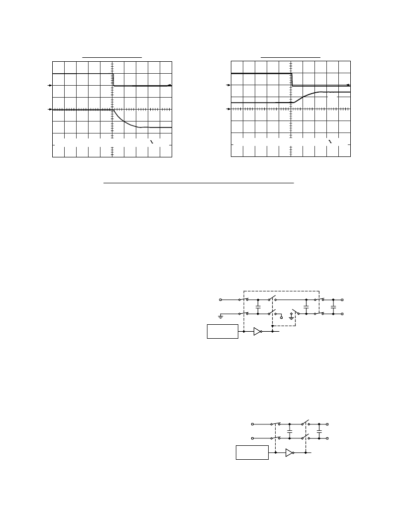
1
T
[
]
Tek Stop 500kS/s
101 Acqs
T
T
SD
2
Ch1 5.00V Ch2 5.00V M 100 s Ch1 0V
V
–
Figure 13. Charge Pump V– Exiting Shutdown
1
T
[
]
Tek Stop 500kS/s
244 Acqs
T
SD
2
V+
Ch1 5.00V Ch2 5.00V M 100 s Ch1 0V
T
Figure 14. Charge Pump V+ Exiting Shutdown
相關PDF資料 |
PDF描述 |
|---|---|
| ADM3311EARS-REEL | 15 kV ESD Protected, 2.7 V to 3.6 V Serial Port Transceivers with Green Idle⑩ |
| ADM3311EARS-Reel25 | 15 kV ESD Protected, +2.7 V to +3.6 V Serial Port Transceiver with Green Idle⑩ |
| ADM3311EARS-REEL7 | 15 kV ESD Protected, 2.7 V to 3.6 V Serial Port Transceivers with Green Idle⑩ |
| ADM3311EARU | 15 kV ESD Protected, 2.7 V to 3.6 V Serial Port Transceivers with Green Idle⑩ |
| ADM3311EARU-REEL | 15 kV ESD Protected, 2.7 V to 3.6 V Serial Port Transceivers with Green Idle⑩ |
相關代理商/技術參數 |
參數描述 |
|---|---|
| ADM3311EARSQ9 | 制造商:Analog Devices 功能描述: |
| ADM3311EARS-REEL | 功能描述:IC TXRX RS-232 3:5 2.7V 28SSOP RoHS:否 類別:集成電路 (IC) >> 接口 - 驅動器,接收器,收發器 系列:- 標準包裝:121 系列:- 類型:收發器 驅動器/接收器數:1/1 規程:RS422,RS485 電源電壓:3 V ~ 3.6 V 安裝類型:表面貼裝 封裝/外殼:10-WFDFN 裸露焊盤 供應商設備封裝:10-DFN(3x3) 包裝:管件 |
| ADM3311EARS-REEL2.5 | 制造商:未知廠家 制造商全稱:未知廠家 功能描述:Transceiver |
| ADM3311EARS-REEL25 | 制造商:AD 制造商全稱:Analog Devices 功能描述:15 kV ESD Protected, +2.7 V to +3.6 V Serial Port Transceiver with Green Idle⑩ |
| ADM3311EARS-REEL7 | 功能描述:IC TXRX RS-232 3:5 2.7V 28SSOP RoHS:否 類別:集成電路 (IC) >> 接口 - 驅動器,接收器,收發器 系列:- 標準包裝:121 系列:- 類型:收發器 驅動器/接收器數:1/1 規程:RS422,RS485 電源電壓:3 V ~ 3.6 V 安裝類型:表面貼裝 封裝/外殼:10-WFDFN 裸露焊盤 供應商設備封裝:10-DFN(3x3) 包裝:管件 |
發布緊急采購,3分鐘左右您將得到回復。