- 您現在的位置:買賣IC網 > PDF目錄374005 > ADM660AR (ANALOG DEVICES INC) CMOS Switched-Capacitor Voltage Converters PDF資料下載
參數資料
| 型號: | ADM660AR |
| 廠商: | ANALOG DEVICES INC |
| 元件分類: | 穩壓器 |
| 英文描述: | CMOS Switched-Capacitor Voltage Converters |
| 中文描述: | SWITCHED CAPACITOR CONVERTER, 120 kHz SWITCHING FREQ-MAX, PDSO8 |
| 封裝: | MS-012AA, SOIC-8 |
| 文件頁數: | 6/8頁 |
| 文件大小: | 111K |
| 代理商: | ADM660AR |
ADM660/ADM8660
REV. A
–6–
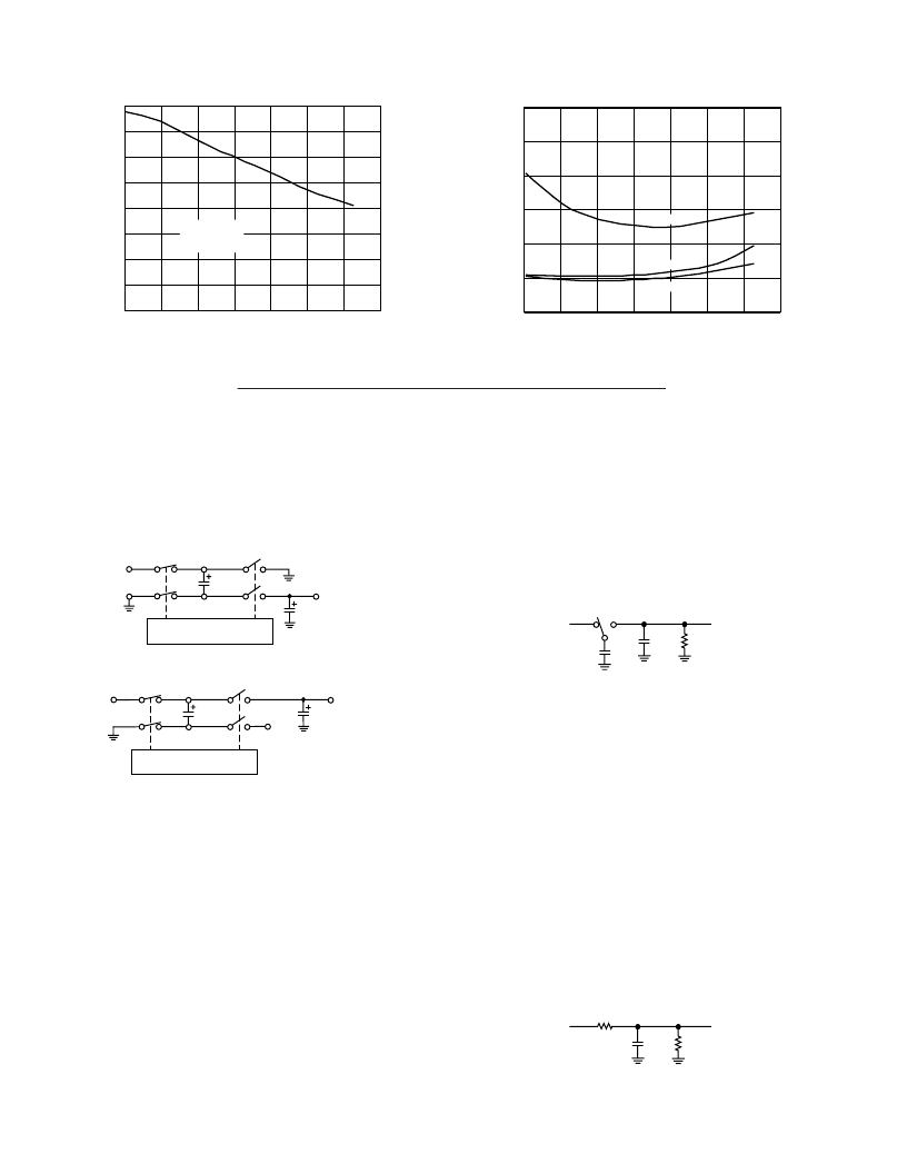
TEMPERATURE –
°
C
–40
C
100
–20
0
20
40
60
80
160
0
140
80
60
40
20
120
100
LV = GND
FC = V+
C1, C2 = 2.2μF
Figure 13. Charge-Pump Frequency vs. Temperature
TEMPERATURE –
°
C
60
O
0
–40
100
–20
0
20
40
60
80
50
40
30
20
10
V+ = +1.5V
V+ = +3V
V+ = +5V
Figure 14. Output Resistance vs. Temperature
GE NE RAL INFORMAT ION
T he ADM660/ADM8660 is a switched capacitor voltage con-
verter that can be used to invert the input supply voltage. T he
ADM660 can also be used in a voltage doubling mode. T he
voltage conversion task is achieved using a switched capacitor
technique using two external charge storage capacitors. An on-
board oscillator and switching network transfers charge between
the charge storage capacitors. T he basic principle behind the
voltage conversion scheme is illustrated in Figures 15 and 16.
C2
CAP+
C1
CAP–
S3
S4
S1
S2
OUT = –V+
V+
Φ
1
Φ
2
÷
2
OSCILLATOR
Figure 15. Voltage Inversion Principle
C2
CAP+
C1
CAP–
S3
S4
S1
S2
Φ
1
Φ
2
V
OUT
= 2V+
V+
V+
÷
2
OSCILLATOR
Figure 16. Voltage Doubling Principle
Figure 15 shows the voltage inverting configuration, while Figure
16 shows the configuration for voltage doubling. An oscillator
generating antiphase signals
φ
1 and
φ
2 controls switches S1, S2
and S3, S4. During
φ
1, switches S1 and S2 are closed charging
C1 up to the voltage at V+. During
φ
2, S1 and S2 open and S3
and S4 close. With the voltage inverter configuration during
φ
2,
the positive terminal of C1 is connected to GND via S3 and the
negative terminal of C1 connects to V
OUT
via S4. T he net result
is voltage inversion at V
OUT
wrt GND. Charge on C1 is trans-
ferred to C2 during
φ
2. Capacitor C2 maintains this voltage
during
φ
1. T he charge transfer efficiency depends on the on-
resistance of the switches, the frequency at which they are being
switched and also on the equivalent series resistance (ESR) of
the external capacitors. T he reason for this is explained in the
following section. For maximum efficiency, capacitors with low
ESR are, therefore, recommended.
T he voltage doubling configuration reverses some of the con-
nections but the same principle applies.
Switched Capacitor T heory of Operation
As already described, the charge pump on the ADM660/
ADM8660 uses a switched capacitor technique in order to
invert or double the input supply voltage. Basic switched
capacitor theory is discussed below.
A switched capacitor building block is illustrated in Figure 17.
With the switch in position A, capacitor C1 will charge to volt-
age V1. T he total charge stored on C1 is q1 = C1V1. T he
switch is then flipped to position B discharging C1 to voltage
V2. T he charge remaining on C1 is q2 = C1V2. T he charge
transferred to the output V2 is, therefore, the difference be-
tween q1 and q2, so
q = q1–q2 = C1 (V1–V2).
C1
A
B
C2
R
L
V1
V2
Figure 17. Switched Capacitor Building Block
As the switch is toggled between A and B at a frequency f, the
charge transfer per unit time or current is
I
=
f
(
q
)
=
f
(
C
1)(
V
1±
V
2)
T herefore
I
=
(
V
1±
V
2)/(1/
fC
1)
=
(
V
1±
V
2)/(
R
EQ
)
where
R
EQ
= 1/fC1
T he switched capacitor may, therefore, be replaced by an
equivalent resistance whose value is dependent on both the
capacitor size and the switching frequency. T his explains why
lower capacitor values may be used with higher switching fre-
quencies. It should be remembered that as the switching fre-
quency is increased the power consumption will increase due to
some charge being lost at each switching cycle. As a result, at high
frequencies the power efficiency starts decreasing. Other losses
include the resistance of the internal switches and the equivalent
series resistance (ESR) of the charge storage capacitors.
C2
R
L
V1
V2
R
EQ
R
EQ
= 1/fC1
Figure 18. Switched Capacitor Equivalent Circuit
相關PDF資料 |
PDF描述 |
|---|---|
| ADM8660AR | CMOS Switched-Capacitor Voltage Converters |
| ADM660ARU | CMOS Switched-Capacitor Voltage Converters |
| ADM663 | Tri-Mode: +3.3 V, +5 V, Adjustable Micropower Linear Voltage Regulators |
| ADM663A | Tri-Mode: +3.3 V, +5 V, Adjustable Micropower Linear Voltage Regulators |
| ADM663AAN | Tri-Mode: +3.3 V, +5 V, Adjustable Micropower Linear Voltage Regulators |
相關代理商/技術參數 |
參數描述 |
|---|---|
| ADM660AR-REEL | 制造商:Rochester Electronics LLC 功能描述:CHARGE PUMPED INVERTER I.C. - Tape and Reel 制造商:Analog Devices 功能描述:IC,DC/DC CONVERTER,CMOS,SOP,8PIN |
| ADM660AR-REEL7 | 制造商:Analog Devices 功能描述:Charge Pump INV/STPUP -1.5V to -7V/5V to 14V 100mA 8-Pin SOIC N T/R |
| ADM660ARU | 制造商:Analog Devices 功能描述:Charge Pump INV/STPUP -1.5V to -7V/5V to 14V 100mA 16-Pin TSSOP 制造商:Rochester Electronics LLC 功能描述:CHARGE PUMPED INVERTER I.C. - Bulk |
| ADM660ARU-REEL | 制造商:Analog Devices 功能描述:Charge Pump INV/STPUP -1.5V to -7V/5V to 14V 100mA 16-Pin TSSOP T/R 制造商:Rochester Electronics LLC 功能描述:CHARGE PUMPED INVERTER I.C. - Tape and Reel |
| ADM660ARU-REEL7 | 制造商:Analog Devices 功能描述:Charge Pump INV/STPUP -1.5V to -7V/5V to 14V 100mA 16-Pin TSSOP T/R 制造商:Rochester Electronics LLC 功能描述:CHARGE PUMPED INVERTER I.C. - Tape and Reel |
發布緊急采購,3分鐘左右您將得到回復。