- 您現在的位置:買賣IC網 > PDF目錄374015 > ADM8694 (Analog Devices, Inc.) bqTINY(TM) Linear 1-cell Li-Ion Charger w/ 1-A FET, Charge Enable & Term Enable in QFN-10 10-SON -40 to 85 PDF資料下載
參數資料
| 型號: | ADM8694 |
| 廠商: | Analog Devices, Inc. |
| 英文描述: | bqTINY(TM) Linear 1-cell Li-Ion Charger w/ 1-A FET, Charge Enable & Term Enable in QFN-10 10-SON -40 to 85 |
| 中文描述: | 微處理器監控電路 |
| 文件頁數: | 8/16頁 |
| 文件大小: | 183K |
| 代理商: | ADM8694 |
ADM8690–ADM8695
REV. 0
–8–
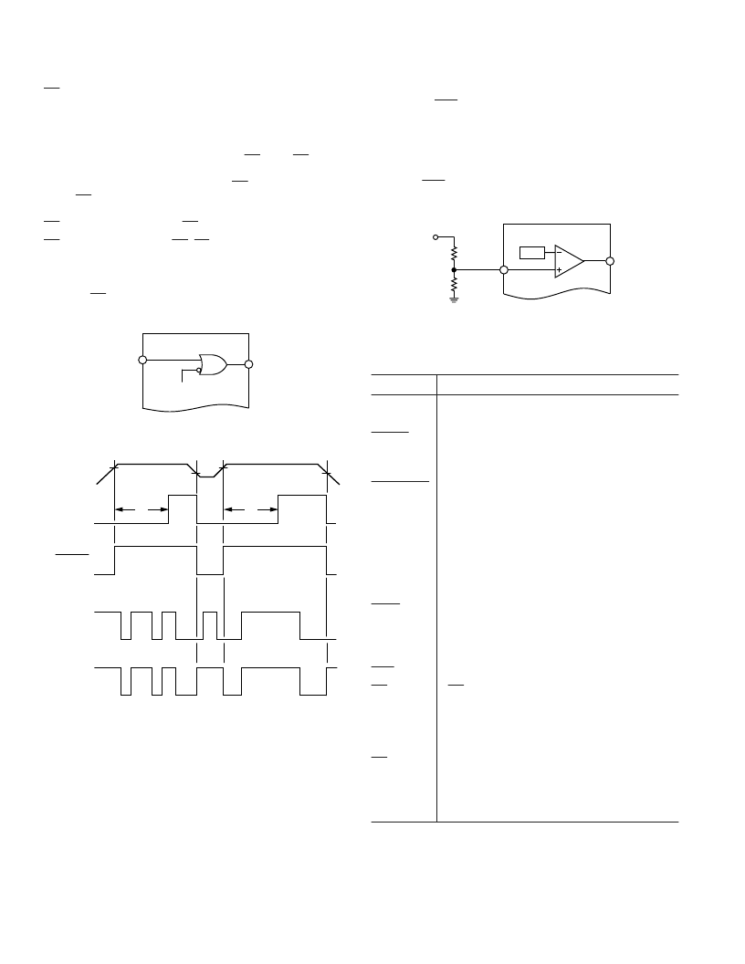
(PFI) is compared to an internal +1.3 V reference. T he Power
Fail Output (
PFO
) goes low when the voltage at PFI is less than
1.3 V. T ypically PFI is driven by an external voltage divider that
senses either the unregulated dc input to the system’s 5 V regu-
lator or the regulated 5 V output. T he voltage divider ratio can
be chosen such that the voltage at PFI falls below 1.3 V several
milliseconds before the +5 V power supply falls below the reset
threshold.
PFO
is normally used to interrupt the microprocessor
so that data can be stored in RAM and the shut down procedure
executed before power is lost
ADM869x
1.3V
POWER
FAIL
OUTPUT
POWER
FAIL
INPUT
PFO
R1
R2
INPUT
POWER
Figure 7. Power Fail Comparator
T able II. Input and Output Status In Battery Backup Mode
Signal
Status
V
OUT
V
OUT
is connected to V
BAT T
via an internal
PMOS switch.
Logic low.
Logic high. T he open circuit output voltage is
equal to V
OUT
.
Logic low.
Logic high. T he open circuit voltage is equal to
V
OUT .
WDI is ignored. It is internally disconnected
from the internal pull-up resistor and does not
source or sink current as long as its input voltage
is between GND and V
OUT
. T he input voltage
does not affect supply current.
Logic high. T he open circuit voltage is equal
to V
OUT
.
T he Power Fail Comparator is turned off and
has no effect on the Power Fail Output.
Logic low.
CE
IN
is ignored. It is internally disconnected
from its internal pull-up and does not source or
sink current as long as its input voltage is
between GND and V
OUT
. T he input voltage
does not affect supply current.
Logic high. T he open circuit voltage is equal to
V
OUT
.
OSC IN is ignored.
OSC SEL is ignored.
RESET
RESET
LOW LINE
BAT T ON
WDI
WDO
PFI
PFO
CE
IN
CE
OUT
OSC IN
OSC SEL
CE
Gating and RAM Write Protection (ADM8691/ADM8693/
ADM8695)
T he ADM8691/ADM8693/ADM8695 products include
memory protection circuitry which ensures the integrity of data
in memory by preventing write operations when V
CC
is at an in-
valid level. T here are two additional pins,
CE
IN
and
CE
OUT
,
which may be used to control the Chip Enable or Write inputs
of CMOS RAM. When V
CC
is present,
CE
OUT
is a buffered rep-
lica of
CE
IN
, with a 3 ns propagation delay. When V
CC
falls be-
low the reset voltage threshold or V
BAT T
, an internal gate forces
CE
OUT
high, independent of
CE
IN
.
CE
OUT
typically drives the
CE
,
CS
or write input of battery
backed up CMOS RAM. T his ensures the integrity of the data
in memory by preventing write operations when V
CC
is at an in-
valid level. Similar protection of EEPROMs can be achieved by
using the
CE
OUT
to drive the store or write inputs.
ADM869x
CE
IN
CE
OUT
V
CC
LOW = 0
V
CC
OK = 1
Figure 5. Chip Enable Gating
V
CC
RESET
LOW LINE
t
1
t
1
t
1
= RESET TIME
V1 = RESET VOLTAGE THRESHOLD LOW
V2 = RESET VOLTAGE THRESHOLD HIGH
HYSTERESIS = V2–V1
V1
V2
V2
V1
CE
IN
CE
OUT
Figure 6. Chip Enable Timing
Power Fail Warning Comparator
An additional comparator is provided for early warning of fail-
ure in the microprocessor’s power supply. T he Power Fail Input
相關PDF資料 |
PDF描述 |
|---|---|
| ADM8694AN | bqTINY(TM) Linear 1-cell Li-Ion Charger w/ 1-A FET, Temp Sense & Charge Enable in QFN-10 10-SON -40 to 85 |
| ADM8694ARN | Single Chip Li-Ion Charge Management IC for Handheld Applications (bqTINY) 10-SON -40 to 125 |
| ADM8690-ADM8695 | Microprocessor Supervisory Circuits |
| ADM8690 | Microprocessor Supervisory Circuits(微處理器監控電路) |
| ADM8690ADM8695 | Microprocessor Supervisory Circuits |
相關代理商/技術參數 |
參數描述 |
|---|---|
| ADM8694AN | 制造商:Analog Devices 功能描述:Processor Supervisor 4.65V 4.75V to 5.5V 8-Pin PDIP 制造商:Rochester Electronics LLC 功能描述:IMPROVED ADM694 - Bulk |
| ADM8694ANZ | 制造商:Analog Devices 功能描述:Processor Supervisor 4.65V 4.75V to 5.5V 8-Pin PDIP 制造商:Analog Devices 功能描述:SUPERVISOR MICROPROCESSOR PDIP8 |
| ADM8694ARN | 制造商:Analog Devices 功能描述:Processor Supervisor 4.65V 4.75V to 5.5V 8-Pin SOIC N 制造商:Rochester Electronics LLC 功能描述:IMPROVED ADM694 - Bulk |
| ADM8694ARN-REEL | 制造商:Analog Devices 功能描述:Processor Supervisor 4.65V 4.75V to 5.5V 8-Pin SOIC N T/R 制造商:Rochester Electronics LLC 功能描述:IMPROVED ADM694 - Tape and Reel |
| ADM8694ARNZ | 制造商:Analog Devices 功能描述:Processor Supervisor 4.65V 4.75V to 5.5V 8-Pin SOIC N 制造商:Analog Devices 功能描述:Microprocessor Supervisor |
發布緊急采購,3分鐘左右您將得到回復。