- 您現(xiàn)在的位置:買賣IC網(wǎng) > PDF目錄374016 > ADM8840 (Analog Devices, Inc.) Charge Pump Regulator & COM Driver for Color TFT Panel PDF資料下載
參數(shù)資料
| 型號: | ADM8840 |
| 廠商: | Analog Devices, Inc. |
| 英文描述: | Charge Pump Regulator & COM Driver for Color TFT Panel |
| 中文描述: | 電荷泵穩(wěn)壓器 |
| 文件頁數(shù): | 6/10頁 |
| 文件大小: | 166K |
| 代理商: | ADM8840 |
ADM8840
–6–
REV. PrG
2/03
PRELIMINARY TECHNICAL DATA
19
ADD_OUT
Voltage Adder Output Pin. This is voltage generated by adding VOUT
(unregulated output of first stage doubler) to V
CC
. This summed voltage is
then used as the supply for the gain stage which generates the Level
Translator Output Voltage. A 4.7 F capacitor is recommended for this pin.
20,21
C5+,C5-
External capacitor C5 is connected between these pins. A 3.3 F capacitor is
recommended.
23
+15VOUT
+15.0V output pin. This was derived by tripling the +5.0V regulated output. A
0.22 F capacitor is required on this pin.
29,28
C4+,C4-
External capacitor C4 is connected between these pins. A 0.22 F capacitor is
recommended.
25,24
C3+,C3-
External capacitor C3 is connected between these pins. A 0.22 F capacitor is
recommended.
27,26
C2+,C2-
External capacitor C2 is connected between these pins. A 0.22 F capacitor is
recommended.
30
-15VOUT
-15.0V output pin. This was derived by inverting the +15.0V output. A
0.22 F capacitor is required on this pin.
PIN FUNCTION DESCRIPTION (Contd.)
Pin
Mnemonic
Function
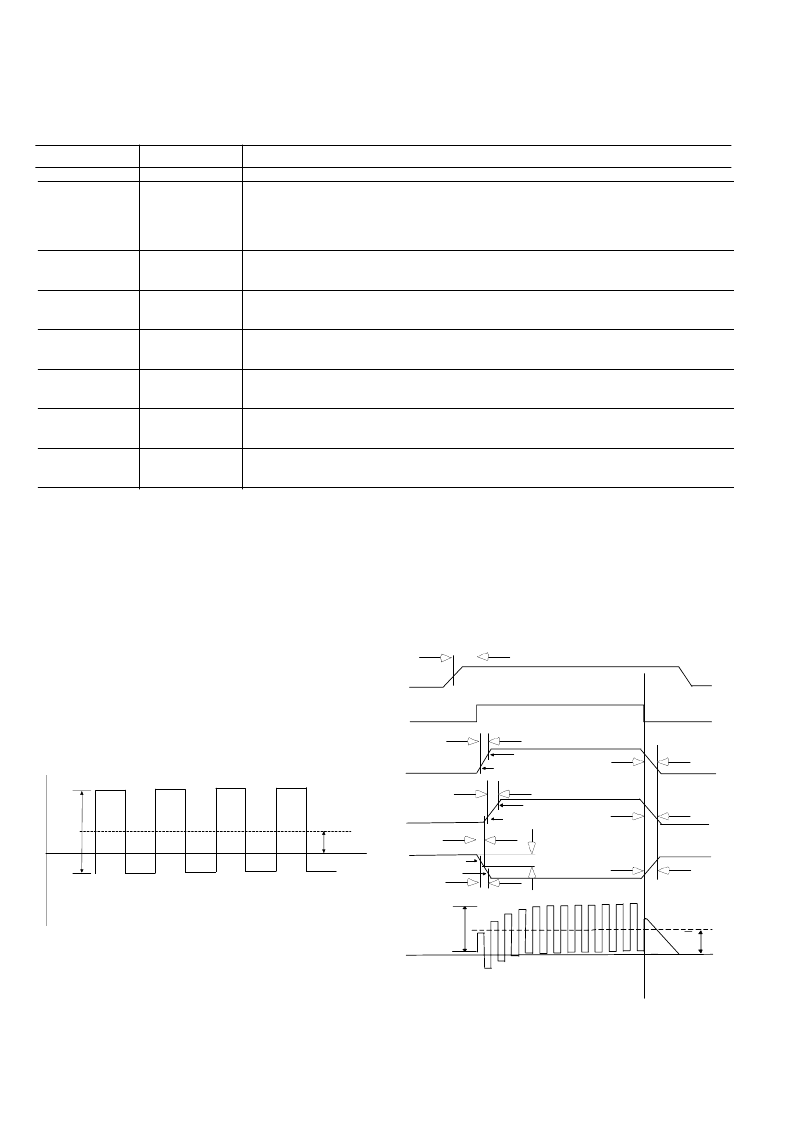
COM_OUT VOLTAGE
The COM Driver section of the ADM8840 can be used to
generate the alternate frame or line inversion of the COM
line of the LCD panel. The ADM8840 receives the COM
clock (with frequency up to 10kHz) from the controller and
allows programmable conditioning of its amplitude and
centre voltage through the use of on-board DAC’s 1 and 2.
This allows programmable elimination of display flicker
caused by the COM inversion.
The COM_OUT amplitude can be programmed from 4.0V
to 7.0V in steps of 28mV. The COM_OUT centre voltage
can be programmed from 0.9V to 2.8V in steps of 14mV.
Figure 1 below shows a typical output from the COM_OUT
pin. If programmable operation is not required the DACs can
be shutdown with the DAC1_SD and DAC2_SD pins and an
analog voltage applied to the DAC1_IN and DAC2_IN pins
to set up the amplitude and centre voltage at COM_OUT.
0.9V->1.8V->2.8V
4.0Vto7.0V
0V
Figure 1. COM_OUT Voltage
Figure 2. Power Sequence
POWER SEQUENCING
In order for the TFT panel to power up correctly, the gate
drive supplies must be sequenced such that the -15V supply
starts up before the +15V supply. The ADM8840 controls
this sequence. When the device is turned on, the ADM8840
allow the -15V output to ramp immediately, but holds off the
+15V output. It continues to do this until the negative output
has reached -3V. At this point, the positive output is enabled
and allowed to ramp to +15V. This sequence is highlighted
in figure 2.
V
CC
SHDN
+5V
+15V
-15V
-3V
t
FM15V
t
RM15V
t
F15V
t
F5V
t
R5V
t
R15V
t
DELAY2
90%
10%
90%
10%
90%
10%
t
DELAY1
CENTRE
0.VOLTAGE:
AMPLITUDE:
0V
COM_OUT
相關(guān)PDF資料 |
PDF描述 |
|---|---|
| ADM8840ACP | 20-17 (6 Contacts) Socket Insert; For Use With:Amphenol MIL-C-5015 97 Series Circular Connectors; No. of Contacts:6 |
| ADM8845 | Charge Pump Driver for LCD White LED Backlights |
| ADM8845ACP | Charge Pump Driver for LCD White LED Backlights |
| ADM8845ACP-REEL7 | Charge Pump Driver for LCD White LED Backlights |
| ADM8845ACPZ | Charge Pump Driver for LCD White LED Backlights |
相關(guān)代理商/技術(shù)參數(shù) |
參數(shù)描述 |
|---|---|
| ADM8840ACP | 制造商:Analog Devices 功能描述:LCD DRVR 2.7V TO 3.6V 32LFCSP - Bulk |
| ADM8840ACP-REEL7 | 制造商:Analog Devices 功能描述: |
| ADM8843 | 制造商:AD 制造商全稱:Analog Devices 功能描述:4 White LED Backlight Driver |
| ADM8843ACPZ | 制造商:Analog Devices 功能描述:LED DRVR 4SEGMENT 3.3V/5V 16LFCSP EP - Bulk |
| ADM8843ACPZ1-R7 | 制造商:Analog Devices 功能描述: |
發(fā)布緊急采購,3分鐘左右您將得到回復。