- 您現(xiàn)在的位置:買賣IC網(wǎng) > PDF目錄374017 > ADN2843CHIPSET-B (ANALOG DEVICES INC) 10.709 Gbps Laser Diode Driver Chipset PDF資料下載
參數(shù)資料
| 型號: | ADN2843CHIPSET-B |
| 廠商: | ANALOG DEVICES INC |
| 元件分類: | 其它接口 |
| 英文描述: | 10.709 Gbps Laser Diode Driver Chipset |
| 中文描述: | SPECIALTY INTERFACE CIRCUIT, UUC |
| 封裝: | DIE |
| 文件頁數(shù): | 6/12頁 |
| 文件大小: | 710K |
| 代理商: | ADN2843CHIPSET-B |
REV. 0
–6–
ADN2843
GENERAL
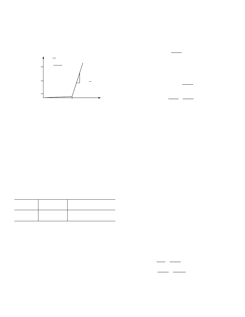
Laser diodes have current-in to light-out transfer functions as
shown in Figure 1. Two key characteristics of this transfer function
are the threshold current, I
TH
, and slope in the linear region
beyond the threshold current, referred to as the slope efficiency, LI.
ER = P1
P0
2
I
TH
CURRENT
O
P0
P1
P
AV
P
I
I
LI =
P
P
AV
= P1 + P0
Figure 1. Laser Transfer Function
CONTROL
A monitor photodiode, MPD, is required to control the LD. The
MPD current is fed into the ADN2843 to control the power
and extinction ratio, continuously adjusting the bias current and
modulation current in response to the laser’s changing threshold
current and light-to-current slope efficiency.
The ADN2843 uses automatic power control, APC, to maintain
a constant average power over time and temperature.
The ADN2843 uses closed-loop extinction ratio control to allow
optimum setting of the extinction ratio for every device. Thus,
SONET/SDH interface standards can be met over device variation,
temperature, and laser aging. Closed-loop modulation control
eliminates the need to either overmodulate the LD or include
external components for temperature compensation, thus reducing
research and development time and second sourcing issues.
The ADN2843 dual-loop control has two modes of operation.
Each mode is given by the configuration of the MODE and
D_IMOD pins as shown below.
Operation
Mode
MODE
Pin Setting
D_IMOD
Pin Connected to
A
B
HIGH
LOW
IBIAS
IBIAS_CTRL
Configuring the ADN2843 in Mode A or Mode B (see Figures 3
and 4) enables users to achieve accurate control of the extinc-
tion ratio. Mode B is suitable for applications where an IBIAS
pin is not available to the TOSA, or where there is no space
on the TOSA for an IBIAS inductor. Experimental data and
simulation for typical lasers has shown ER to be 0.3 dB to 0.5 dB
better in Mode A, at a 5 dB extinction ratio. Care should be
taken to ensure that the extra capacitance on the I
BIAS
pin
due to the D_IMOD connection does not degrade the eye
quality. When physical constraints do not allow a low capaci-
tance interconnect between D_IMOD and I
BIAS
, the ADN2843
should be configured in Mode B (see Figure 4).
Average power and extinction ratio for both modes are set using
the PSET and ERSET pins, respectively. Potentiometers are
connected between these pins and ground. The potentiometer
R
PSET
is used to set the average power. The potentiometer R
ERSET
is used to set the extinction ratio. The internal control loops
force the PSET and ERSET pins to 1.23 V above GND. For
initial setup, R
PSET
and R
ERSET
may be calculated using the
following formulas:
The PSET resistor is given by the following formulas:
R
V
I
PSET
AV
=
( )
1 23
.
W
where
I
AV
is average MPD current.
The value of the ERSET resistor is a function of the operation
mode of the ADN2843 as follows:
For Mode A:
R
R
ER
ER
ERSET
PSET
=
¥
+
1
–
1
For Mode B:
R
R
ER
ER
ERSET
PSET
2
=
¥
+
–
1
1
Note that I
ERSET
and I
PSET
will change from laser diode to laser
diode, therefore R
ERSET
and R
PSET
need to be adjusted for each
laser diode. When tuning the laser diode, R
PSET
should be
adjusted first with R
ERSET
at 25 k . Once the average power is
set, R
ERSET
is adjusted to set the desired extinction ratio, and
R
PSET
is again adjusted to re-establish the desired average power.
Once the values R
PSET
and R
ERSET
have been adjusted to set the
desired average power and extinction ratio, the control loops
maintain these values of average power and extinction ratio over
environmental conditions and time.
PAVCAP AND ERCAP
The control loop constants are set by the PAVCAP and ERCAP
capacitors. The required value for the PAVCAP and ERCAP
capacitors is 22 nF.
The PAVCAP and ERCAP capacitors are connected between
the respective pins and GND. The capacitors should be low
leakage multilayer ceramic capacitors with an insulation resistance
>100 G or an RC >1000 s, whichever is lowest.
ALARMS
The ADN2843 is designed to allow interface compliance to
ITU-T-G958 (11/94), Section 10.3.1.1.2 (Transmitter Fail),
and Section 10.3.1.1.3 (transmitter degrade). The ADN2843
has two alarms, DEGRADE and FAIL. These alarms are raised
when I
BIAS
exceeds the respective DEGRADE and FAIL thresh-
olds. These alarms are active high. A resistor between ground
and the ASET pin is used to set the current at which these
alarms are raised. The current through the ASET resistor is a
ratio of 1:100 to the FAIL alarm threshold. The DEGRADE
alarm will be raised at 90% of the FAIL threshold.
Example:
I
mA so I
I
ASET
=
100
100
1 23
.
mA
I
mA
A
R
V
I
V
A
k
FAIL
DEGRADE
50
FAIL
ASET
ASET
=
=
=
=
=
=
=
50
45
500
1 23
500
2 46
.
.
W
The laser degrade alarm, DEGRADE, is provided to give a warn-
ing of imminent laser failure if the laser diode degrades further or
if environmental conditions continue to stress the LD, such as
increasing temperature.
相關(guān)PDF資料 |
PDF描述 |
|---|---|
| ADN2847 | 3 V Dual-Loop 50 Mbps to 3.3 Gbps Laser Diode Driver |
| ADN2847ACP-32 | 3 V Dual-Loop 50 Mbps to 3.3 Gbps Laser Diode Driver |
| ADN2847ACP-32-RL | 3 V Dual-Loop 50 Mbps to 3.3 Gbps Laser Diode Driver |
| ADN2847ACP-32-RL7 | 3 V Dual-Loop 50 Mbps to 3.3 Gbps Laser Diode Driver |
| ADN2847ACP-48 | 3 V Dual-Loop 50 Mbps to 3.3 Gbps Laser Diode Driver |
相關(guān)代理商/技術(shù)參數(shù) |
參數(shù)描述 |
|---|---|
| ADN2844BCP-32 | 制造商:Analog Devices 功能描述: |
| ADN2847 | 制造商:Analog Devices 功能描述: |
| ADN2847ACP-32 | 制造商:Analog Devices 功能描述:Laser Driver DFB 3.3Gbps 1-CH 32-Pin LFCSP EP |
| ADN2847ACP-32-RL | 制造商:Analog Devices 功能描述:Laser Driver DFB 3.3Gbps 1-CH 32-Pin LFCSP EP T/R |
| ADN2847ACP-32-RL7 | 制造商:Analog Devices 功能描述:Laser Driver DFB 3.3Gbps 1-CH 32-Pin LFCSP EP T/R |
發(fā)布緊急采購,3分鐘左右您將得到回復(fù)。