- 您現(xiàn)在的位置:買賣IC網(wǎng) > PDF目錄374017 > ADN2849 (Analog Devices, Inc.) 10.7 Gbps Electro-Absorption Modulator Driver PDF資料下載
參數(shù)資料
| 型號(hào): | ADN2849 |
| 廠商: | Analog Devices, Inc. |
| 英文描述: | 10.7 Gbps Electro-Absorption Modulator Driver |
| 中文描述: | 10.7 Gbps的電吸收調(diào)制器驅(qū)動(dòng) |
| 文件頁(yè)數(shù): | 15/17頁(yè) |
| 文件大小: | 1425K |
| 代理商: | ADN2849 |
第1頁(yè)第2頁(yè)第3頁(yè)第4頁(yè)第5頁(yè)第6頁(yè)第7頁(yè)第8頁(yè)第9頁(yè)第10頁(yè)第11頁(yè)第12頁(yè)第13頁(yè)第14頁(yè)當(dāng)前第15頁(yè)第16頁(yè)第17頁(yè)
Preliminary Technical Data
ADN2849
APPLICATIONS INFORMATION
Rev. Pr. G | Page 15 of 17
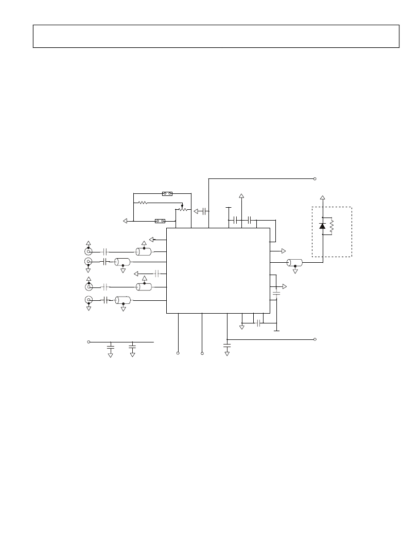
TYPICAL APPLICATION CIRCUIT
Figure 31 shows the typical application circuit for the
ADN2849. Applying DC voltages to the BIAS_SET and
MOD_SET pins can control the Modulation and bias offset
voltages. The data signal source must be connected to the
DATAP and DATAN pins using 50
impedance transmission
lines. If a reference clock signal is available, the retiming option
can be enabled using the CLK_SELB input. Note that the
connection between the clock signal source and
the CLKP and CLKN pins must be made using
50
transmission lines. The cross point can be adjusted using
the potentiometer R3. The modulation voltage can be enabled
or disabled using the MOD_ENB pin.
The ADN2849 can operate with positive or negative (5.0V or
5.2V) supply voltage. Care should be taken to connect the GND
pins to the positive rail of the supply voltage while the VEE and
the exposed pad to the negative rail of the supply voltage.
MOD_ENB
CLK_SELB
GND GND
GND
DATAP
DATAN
ADN2849
U1
VBB
CLKP
CLKN
VEE
VTERM
GND
MODP
MODN_TERM
GND
VEE
CPAN CPAP
BIAS_SET
VEE
GND VTERM
J1
C1
C2
GND
GND
Z0=50
Z0=50
J2
J3
C3
C4
GND
GND
Z0=50
Z0=50
J4
C7
JP2
R3
R4
JP1
C15
BIAS_SET
C18
C13
Z0=50
C11
C10
MOD_SET
C12
MOD_SET
CLK_SELB
MOD_ENB
GND
GND
GND
GND
GND
GND
GND
GND
VEE
GND
GND
GND
VEE
GND
GND
GND
C5
C6
VEE
GND
GND
-5.2V
50
EAM
GND
Figure 31. Typical ADN2849 application circuit
PCB LAYOUT GUIDELINES
Due to the high frequencies at which the ADN2849 operates,
care should be taken when designing the PCB layout in order to
obtain optimum performance. It is recommended to use
controlled impedance transmission lines for the high-speed
signal paths The length of the transmission lines must be kept
to a minimum to reduce losses and pattern dependant jitter. All
the VEE and GND pins must be connected to solid copper
planes using low inductance connections. When the
connections are made through vias, multiple vias can be
connected in parallel to reduce the parasitic inductance. The
VTERM, VBB, MODN_TERM and VEE pins must be locally
decoupled with high quality capacitors. If proper decoupling
cannot be achieved using a single capacitor, the user can use
multiple capacitors in parallel for each GND pin. A 20
μ
F
tantalum capacitor must be used as general decoupling
capacitor for the entire module The exposed pad should be
connected to the most negative rail of the supply voltage using
filled vias
so that solder does not leak through the vias during
reflow. Using filled vias under the package greatly enhances the
reliability of the connectivity of the exposed pad to the GND
plane during reflow.
相關(guān)PDF資料 |
PDF描述 |
|---|---|
| ADN2849ACP | 10.7 Gbps Electro-Absorption Modulator Driver |
| ADN2849ACP-RL | 10.7 Gbps Electro-Absorption Modulator Driver |
| ADN2849ACP-RL7 | 10.7 Gbps Electro-Absorption Modulator Driver |
| ADN2849SURF | 10.7 Gbps Electro-Absorption Modulator Driver |
| ADN2850ACP25 | Nonvolatile Memory, Dual 1024 Position Programmable Resistors |
相關(guān)代理商/技術(shù)參數(shù) |
參數(shù)描述 |
|---|---|
| ADN2849ACP | 制造商:AD 制造商全稱:Analog Devices 功能描述:10.7 Gbps Electro-Absorption Modulator Driver |
| ADN2849ACP-RL | 制造商:AD 制造商全稱:Analog Devices 功能描述:10.7 Gbps Electro-Absorption Modulator Driver |
| ADN2849ACP-RL7 | 制造商:AD 制造商全稱:Analog Devices 功能描述:10.7 Gbps Electro-Absorption Modulator Driver |
| ADN2849SURF | 制造商:AD 制造商全稱:Analog Devices 功能描述:10.7 Gbps Electro-Absorption Modulator Driver |
| ADN2850 | 制造商:AD 制造商全稱:Analog Devices 功能描述:Nonvolatile Memory, Dual 1024 Position Programmable Resistors |
發(fā)布緊急采購(gòu),3分鐘左右您將得到回復(fù)。