- 您現在的位置:買賣IC網 > PDF目錄374017 > ADN2890ACP-RL (ANALOG DEVICES INC) 3.3 V 2.7 Gb/s Limiting Amplifier PDF資料下載
參數資料
| 型號: | ADN2890ACP-RL |
| 廠商: | ANALOG DEVICES INC |
| 元件分類: | 通信及網絡 |
| 英文描述: | 3.3 V 2.7 Gb/s Limiting Amplifier |
| 中文描述: | SPECIALTY TELECOM CIRCUIT, QCC16 |
| 封裝: | 3 X 3 MM, MO-220-VEED-2, LFCSP-16 |
| 文件頁數: | 9/12頁 |
| 文件大小: | 263K |
| 代理商: | ADN2890ACP-RL |
ADN2890
APPLICATIONS INFORMATION
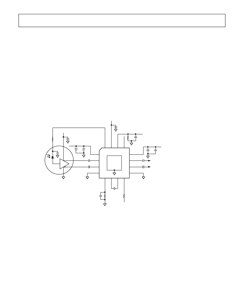
PCB DESIGN GUIDELINES
Proper RF PCB design techniques must be used for optimal
performance.
Power Supply Connections and Ground Planes
Use of one low impedance ground plane is recommended. The
VEE pins should be soldered directly to the ground plane to
reduce series inductance. If the ground plane is an internal
plane and connections to the ground plane are made through
vias, multiple vias can be used in parallel to reduce the series
inductance, especially on Pin 9, which is the ground return for
the output buffers. The exposed pad should be connected to the
GND plane using filled vias
so that solder does not leak through
the vias during reflow. Using filled vias under the package
Rev. 0 | Page 9 of 12
greatly enhances the reliability of the connectivity of the
exposed pad to the GND plane during reflow.
Use of a 10 μF electrolytic capacitor between VCC and VEE is
recommended at the location where the 3.3 V supply enters the
PCB. When using 0.1 μF and 1 nF ceramic chip capacitors, they
should be placed between the IC power supply VCC and VEE,
as close as possible to the ADN2890 VCC pins.
If connections to the supply and ground are made through vias,
the use of multiple vias in parallel helps to reduce series
inductance, especially on Pin 12, which supplies power to the
high speed OUTP/OUTN output buffers. Refer to the schematic
in Figure 8 for recommended connections.
0
CONNECT
EXPOSED
PAD TO
GND
AVCC
1
T
5
C
6
C
7
L
8
P
16
P
15
R
14
S
13
PIN
2
NIN
3
AVEE
4
DRVCC
12
OUTN
10
DRVEE
9
OUTP
C4
C3
11
C2
C1
TO HOST
BOARD
C7
C8
VCC
C5
C6
VCC
C11
C12
R2
200
VCC
R3
4.7k
TO 10k
ON HOST BOARD
VCC
ADN2880
0.1
μ
F
VCC
C9
RSSI MEASUREMENT
TO ADC
R1
C10
C1–C4, C11: 0.01
μ
F X5R/X7R DIELECTRIC, 0201 CASE
C5, C7, C9, C10, C12: 0.1
μ
F X5R/X7R DIELECTRIC, 0402 CASE
C6, C8: 1nF X5R/X7R DIELECTRIC, 0201 CASE
Figure 8. Typical ADN2890 Applications Circuit
相關PDF資料 |
PDF描述 |
|---|---|
| ADN2890ACP-RL7 | 3.3 V 2.7 Gb/s Limiting Amplifier |
| ADN8810 | 12-Bit High Output Current Source |
| ADN8810-EVAL | 12-Bit High Output Current Source |
| ADN8810ACP | 12-Bit High Output Current Source |
| ADN8810ACP-REEL7 | 12-Bit High Output Current Source |
相關代理商/技術參數 |
參數描述 |
|---|---|
| ADN2890ACP-RL7 | 功能描述:IC AMP LIM 16LFCSP RoHS:否 類別:集成電路 (IC) >> Linear - Amplifiers - Instrumentation 系列:- 標準包裝:2,500 系列:- 放大器類型:通用 電路數:1 輸出類型:滿擺幅 轉換速率:0.11 V/µs 增益帶寬積:350kHz -3db帶寬:- 電流 - 輸入偏壓:4nA 電壓 - 輸入偏移:20µV 電流 - 電源:260µA 電流 - 輸出 / 通道:20mA 電壓 - 電源,單路/雙路(±):2.7 V ~ 36 V,±1.35 V ~ 18 V 工作溫度:-40°C ~ 85°C 安裝類型:表面貼裝 封裝/外殼:8-SOIC(0.154",3.90mm 寬) 供應商設備封裝:8-SO 包裝:帶卷 (TR) |
| ADN2890ACPZ-RL | 功能描述:IC AMP LIM 16LFCSP RoHS:是 類別:集成電路 (IC) >> Linear - Amplifiers - Instrumentation 系列:- 標準包裝:50 系列:- 放大器類型:J-FET 電路數:2 輸出類型:- 轉換速率:13 V/µs 增益帶寬積:3MHz -3db帶寬:- 電流 - 輸入偏壓:65pA 電壓 - 輸入偏移:3000µV 電流 - 電源:1.4mA 電流 - 輸出 / 通道:- 電壓 - 電源,單路/雙路(±):7 V ~ 36 V,±3.5 V ~ 18 V 工作溫度:-40°C ~ 85°C 安裝類型:通孔 封裝/外殼:8-DIP(0.300",7.62mm) 供應商設備封裝:8-PDIP 包裝:管件 |
| ADN2890ACPZ-RL7 | 功能描述:IC AMP LIM 16LFCSP RoHS:是 類別:集成電路 (IC) >> Linear - Amplifiers - Instrumentation 系列:- 標準包裝:50 系列:- 放大器類型:J-FET 電路數:2 輸出類型:- 轉換速率:13 V/µs 增益帶寬積:3MHz -3db帶寬:- 電流 - 輸入偏壓:65pA 電壓 - 輸入偏移:3000µV 電流 - 電源:1.4mA 電流 - 輸出 / 通道:- 電壓 - 電源,單路/雙路(±):7 V ~ 36 V,±3.5 V ~ 18 V 工作溫度:-40°C ~ 85°C 安裝類型:通孔 封裝/外殼:8-DIP(0.300",7.62mm) 供應商設備封裝:8-PDIP 包裝:管件 |
| ADN2890XCP | 制造商:Analog Devices 功能描述:- Trays |
| ADN2891 | 制造商:AD 制造商全稱:Analog Devices 功能描述:3.3 V, 3.2 Gbps, Limiting Amplifier |
發布緊急采購,3分鐘左右您將得到回復。