- 您現在的位置:買賣IC網 > PDF目錄8728 > ADN4670BSTZ-REEL7 (Analog Devices Inc)IC CLOCK BUFFER MUX 2:10 32LQFP PDF資料下載
參數資料
| 型號: | ADN4670BSTZ-REEL7 |
| 廠商: | Analog Devices Inc |
| 文件頁數: | 1/12頁 |
| 文件大小: | 0K |
| 描述: | IC CLOCK BUFFER MUX 2:10 32LQFP |
| 標準包裝: | 500 |
| 類型: | 扇出緩沖器(分配),多路復用器 |
| 電路數: | 1 |
| 比率 - 輸入:輸出: | 2:10 |
| 差分 - 輸入:輸出: | 是/是 |
| 輸入: | LVDS |
| 輸出: | LVDS |
| 頻率 - 最大: | 1.1GHz |
| 電源電壓: | 2.375 V ~ 2.625 V |
| 工作溫度: | -40°C ~ 85°C |
| 安裝類型: | 表面貼裝 |
| 封裝/外殼: | 32-LQFP |
| 供應商設備封裝: | 32-LQFP(7x7) |
| 包裝: | 帶卷 (TR) |
Programmable Low Voltage
1:10 LVDS Clock Driver
Data Sheet
Rev. A
Information furnished by Analog Devices is believed to be accurate and reliable. However, no
responsibilityisassumedbyAnalogDevicesforitsuse,norforanyinfringementsofpatentsorother
rightsofthirdpartiesthatmayresultfromitsuse.Specificationssubjecttochangewithoutnotice.No
license is granted by implication or otherwise under any patent or patent rights of Analog Devices.
Trademarksandregisteredtrademarksarethepropertyoftheirrespectiveowners.
One Technology Way, P.O. Box 9106, Norwood, MA 02062-9106, U.S.A.
Tel: 781.329.4700
Fax: 781.461.3113
2010–2012 Analog Devices, Inc. All rights reserved.
FEATURES
Low output skew <30 ps (typical)
Distributes one differential clock input to 10 LVDS clock
outputs
Programmable—one of two differential clock inputs can be
selected (CLK0, CLK1) and individual differential clock
outputs enabled/disabled
Signaling rate up to 1.1 GHz (typical)
2.375 V to 2.625 V power supply range
±100 mV differential input threshold
Input common-mode range from rail-to-rail
I/O pins fail-safe during power-down: VDD = 0 V
Available in 32-lead LFCSP and LQFP packages
Industrial operating temperature range: 40°C to +85°C
APPLICATIONS
Clock distribution networks
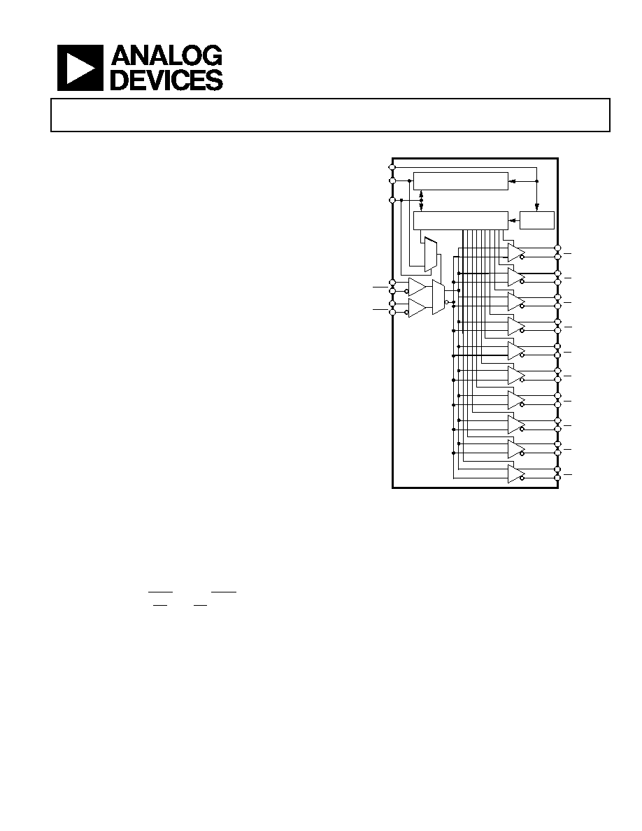
FUNCTIONAL BLOCK DIAGRAM
9 8 7 6 5 4 3 2 1 0
10
12-BIT
COUNTER
11-BIT SHIFT REGISTER
11-BIT CONTROL REGISTER
Q9
Q8
Q7
Q6
Q5
Q4
Q3
Q2
Q1
Q0
CK
SI
EN
CLK0
CLK1
MUX
1
0
CLK0
CLK1
Q9
Q8
Q7
Q6
Q5
Q4
Q3
Q2
Q1
Q0
0
1
08870-
001
Figure 1.
GENERAL DESCRIPTION
The ADN4670 is a low voltage differential signaling (LVDS)
clock driver that expands a differential clock input signal to
10 differential clock outputs. The device is programmable
using a simple serial interface, so that one of two clock inputs
can be selected (CLK0/CLK0 or CLK1/CLK1) and any of the
differential outputs (Q0/Q0 to Q9/Q9) can be enabled or
disabled (tristated). The ADN4670 is designed for use in 50
transmission line environments.
When the enable input EN is high, the device may be pro-
grammed by clocking 11 data bits into the shift register. The
first 10 bits determine which outputs are enabled (0 = disabled,
1 = enabled), while the 11th bit selects the clock input (0 =
CLK0, 1 = CLK1). A 12th clock pulse transfers data from the
shift register to the control register.
The ADN4670 is fully specified over the industrial temperature
range and is available in a 32-lead LFCSP and LQFP packages.
相關PDF資料 |
PDF描述 |
|---|---|
| VE-B1V-MV-F4 | CONVERTER MOD DC/DC 5.8V 150W |
| VE-B1T-MV-F3 | CONVERTER MOD DC/DC 6.5V 150W |
| ADN4670BCPZ-REEL7 | IC CLOCK BUFFER MUX 2:10 16LFCSP |
| VE-B1R-MV-F2 | CONVERTER MOD DC/DC 7.5V 150W |
| VE-B1P-MV-F2 | CONVERTER MOD DC/DC 13.8V 150W |
相關代理商/技術參數 |
參數描述 |
|---|---|
| ADN4690E | 制造商:AD 制造商全稱:Analog Devices 功能描述:3.3 V, 100 Mbps, Half- and Full-Duplex |
| ADN4690EBRZ | 功能描述:IC INTERFACE TXRX RoHS:是 類別:集成電路 (IC) >> 接口 - 驅動器,接收器,收發器 系列:* 標準包裝:98 系列:* |
| ADN4690EBRZ-RL7 | 功能描述:IC TXRX MLVDS 100MBPS 8SOIC RoHS:是 類別:集成電路 (IC) >> 接口 - 驅動器,接收器,收發器 系列:* 標準包裝:121 系列:- 類型:收發器 驅動器/接收器數:1/1 規程:RS422,RS485 電源電壓:3 V ~ 3.6 V 安裝類型:表面貼裝 封裝/外殼:10-WFDFN 裸露焊盤 供應商設備封裝:10-DFN(3x3) 包裝:管件 |
| ADN4691E | 制造商:AD 制造商全稱:Analog Devices 功能描述:3.3 V, 100 Mbps, Half- and Full-Duplex |
| ADN4691EBRZ | 功能描述:IC M-LVDS TRANSCEIVER RoHS:是 類別:集成電路 (IC) >> 接口 - 驅動器,接收器,收發器 系列:* 產品培訓模塊:RS-232 & USB Transceiver 標準包裝:2,000 系列:- 類型:收發器 驅動器/接收器數:1/1 規程:RS232 電源電壓:3 V ~ 5.5 V 安裝類型:表面貼裝 封裝/外殼:16-SSOP(0.209",5.30mm 寬) 供應商設備封裝:16-SSOP 包裝:帶卷 (TR) 其它名稱:296-19849-2 |
發布緊急采購,3分鐘左右您將得到回復。