- 您現在的位置:買賣IC網 > Datasheet目錄39 > ADN8810ACPZ-REEL7 (Analog Devices Inc)IC CURRENT SOURCE(12BIT) 24LFCSP Datasheet資料下載
參數資料
| 型號: | ADN8810ACPZ-REEL7 |
| 廠商: | Analog Devices Inc |
| 文件頁數: | 8/16頁 |
| 文件大小: | 262K |
| 描述: | IC CURRENT SOURCE(12BIT) 24LFCSP |
| 標準包裝: | 1,500 |
| 功能: | 電流源(12 位) |
| 電流 - 輸出: | 300mA |
| 工作溫度: | -40°C ~ 85°C |
| 安裝類型: | 表面貼裝 |
| 封裝/外殼: | 24-VFQFN 裸露焊盤,CSP |
| 供應商設備封裝: | 24-LFCSP-VQ(4x4) |
| 包裝: | 帶卷 (TR) |
ADN8810
Rev. A | Page 8 of 16
ADN8810 TERMINOLOGY
Relative Accuracy
Relative accuracy or integral nonlinearity (INL) is a measure of
the maximum deviation, in least significant bits (LSBs), from an
ideal line passing through the endpoints of the DAC transfer
function. Figure 5 shows a typical INL vs. code plot. The
ADN8810 INL is measured from 2% to 100% of the full-scale
(FS) output.
Differential Nonlinearity
Differential nonlinearity (DNL) is the difference between
the measured change and the ideal 1 LSB change between
any two adjacent codes. A specified differential nonlinearity
of ?1 LSB maximum ensures monotonicity. The ADN8810
is guaranteed monotonic by design. Figure 6 shows a typical
DNL vs. code plot.
Offset Error
Offset error, or zero-code error, is an interpolation of the output
voltage at code 0x000 as predicted by the line formed from the
output voltages at code 0x040 (2% FS) and code 0xFFF (100%
FS). Ideally, the offset error should be 0 V. Offset error occurs
from a combination of the offset voltage of the amplifier and
offset errors in the DAC. It is expressed in LSBs.
Offset Drift
This is a measure of the change in offset error with a change in
temperature. It is expressed in (ppm of full-scale range)/癈.
Gain Error
Gain error is a measure of the span error of the DAC. It is the
deviation in slope of the output transfer characteristic from
ideal. The transfer characteristic is the line formed from the
output voltages at code 0x040 (2% FS) and code 0xFFF (100%
FS). It is expressed as a percent of the full-scale range.
Compliance Voltage
The maximum output voltage from the ADN8810 is a function
of output current and supply voltage. Compliance voltage
defines the maximum output voltage at a given current and
supply voltage to guarantee the device operates within its INL,
DNL, and gain error specifications.
Output Current Change vs. Output Voltage Change
This is a measure of the ADN8810 output impedance and is
similar to a load regulation spec in voltage references. For a
given code, the output current changes slightly as output voltage
increases. It is measured as an absolute value in (ppm of full-
scale range)/V.
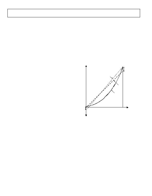
INTERPOLATED
DAC CODE
OFFSET
ERROR
GAIN ERROR
PLUS
OFFSET ERROR
0xFFF
0x040
IDEAL
ACTUAL
(EXAGGERATED)
Figure 4. Output Transfer Function
相關PDF資料 |
PDF描述 |
|---|---|
| ADP2140ACPZ3328R7 | IC REG DL BCK/LINEAR 10LFCSP |
| ADP5022ACBZ-6-R7 | IC REG TRPL BCK/LINEAR 16WLCSP |
| ADP5041ACPZ-1-R7 | IC REG TRPL BCK/LINEAR 20-LFCSP |
| ADP5042ACPZ-2-R7 | IC REG TRPL BCK/LINEAR 20LFCSP |
| ADT6402SRJZ-RL7 | IC TEMP SENS TRIP PT PP SOT-23-6 |
相關代理商/技術參數 |
參數描述 |
|---|---|
| ADN8810-EVAL | 制造商:Analog Devices 功能描述:- Bulk |
| ADN8810XCP | 制造商:Analog Devices 功能描述:- Bulk |
| ADN8820 | 制造商:Analog Devices 功能描述:LASER DRVR 1CH 48LFCSP - Trays |
| ADN8820ACP | 制造商:Analog Devices 功能描述:LASER DRVR 1CH 48LFCSP - Bulk |
| ADN8820-REEL7 | 制造商:AD 制造商全稱:Analog Devices 功能描述:EDFA and CW Laser Controller |
發布緊急采購,3分鐘左右您將得到回復。