- 您現(xiàn)在的位置:買賣IC網(wǎng) > PDF目錄374018 > ADP1111AN-3.3 (ANALOG DEVICES INC) Micropower Step-Up/Step-Down SW Regulator. Adjustable and Fixed 3.3 V 5 V 12 V(406.88 k) PDF資料下載
參數(shù)資料
| 型號: | ADP1111AN-3.3 |
| 廠商: | ANALOG DEVICES INC |
| 元件分類: | 穩(wěn)壓器 |
| 英文描述: | Micropower Step-Up/Step-Down SW Regulator. Adjustable and Fixed 3.3 V 5 V 12 V(406.88 k) |
| 中文描述: | 1.5 A SWITCHING REGULATOR, 88 kHz SWITCHING FREQ-MAX, PDIP8 |
| 封裝: | PLASTIC, DIP-8 |
| 文件頁數(shù): | 12/16頁 |
| 文件大小: | 406K |
| 代理商: | ADP1111AN-3.3 |
ADP1111
–12–
REV. 0
This occurs in the step-up mode when the following condition is
met:
V
OUT
+
V
DIODE
V
IN
V
SW
<
1
1
DC
where DC is the ADP1111’s duty cycle. When this relationship
exists, the inductor current does not go all the way to zero
during the time that the switch is OFF. When the switch turns
on for the next cycle, the inductor current begins to ramp up
from the residual level. If the switch ON time remains constant,
the inductor current will increase to a high level (see Figure 24).
This increases output ripple and can require a larger inductor
and capacitor. By controlling switch current with the I
LIM
resistor, output ripple current can be maintained at the design
values. Figure 25 illustrates the action of the I
LIM
circuit.
Figure 24.
Figure 25.
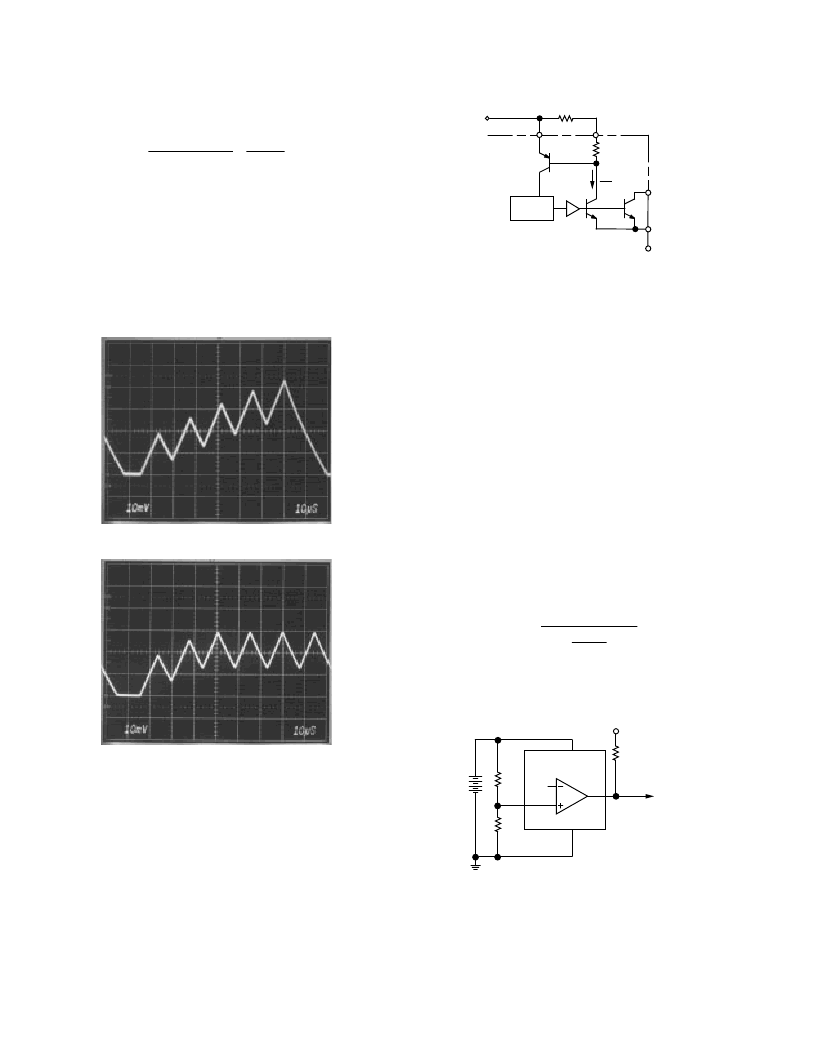
The internal structure of the I
LIM
circuit is shown in Figure 26.
Q1 is the ADP1111’s internal power switch that is paralleled by
sense transistor Q2. The relative sizes of Q1 and Q2 are scaled
so that I
Q2
is 0.5% of I
Q1
. Current flows to Q2 through an
internal 80
resistor and through the R
LIM
resistor. These two
resistors parallel the base-emitter junction of the oscillator-
disable transistor, Q3. When the voltage across R1 and R
LIM
exceeds 0.6 V, Q3 turns on and terminates the output pulse. If
only the 80
internal resistor is used (i.e. the I
LIM
pin is
connected directly to V
IN
), the maximum switch current will be
1.5 A. Figure 6 gives R
LIM
values for lower current-limit values.
72kHz
OSC
V
IN
POWER
SWITCH
SW2
SW1
R
LIM
DRIVER
80
(INTERNAL)
I
LIM
I
Q1
200
V
IN
(EXTERNAL)
Q2
ADP1111
Q1
Q3
R1
Figure 26. ADP1111 Current Limit Operation
The delay through the current limiting circuit is approximately
1
μ
s. If the switch ON time is reduced to less than 3
μ
s, accuracy
of the current trip-point is reduced. Attempting to program a
switch ON time of 1
μ
s or less will produce spurious responses
in the switch ON time; however, the ADP1111 will still provide
a properly regulated output voltage.
PROGRAMMING THE GAIN BLOCK
The gain block of the ADP1111 can be used as a low-battery
detector, error amplifier or linear post regulator. The gain block
consists of an op amp with PNP inputs and an open-collector
NPN output. The inverting input is internally connected to the
ADP1111’s 1.25 V reference, while the noninverting input is
available at the SET pin. The NPN output transistor will sink
about 300
μ
A.
Figure 27a shows the gain block configured as a low-battery
monitor. Resistors R1 and R2 should be set to high values to
reduce quiescent current, but not so high that bias current in
the SET input causes large errors. A value of 33 k
for R2 is a
good compromise. The value for R1 is then calculated from the
formula:
R
1
=
V
LOBATT
1.25
V
1.25
V
R
2
where
V
LOBATT
is the desired low battery trip point. Since the
gain block output is an open-collector NPN, a pull-up resistor
should be connected to the positive logic power supply.
ADP1111
1.25V
REF
SET
GND
AO
5V
R
L
47k
TO
PROCESSOR
R1
R2
V
BAT
V
IN
33k
R1= V
V
LB
= BATTERY TRIP POINT
LB
–1.25V
Figure 27a. Setting the Low Battery Detector Trip Point
200mA/div
200mA/div
相關(guān)PDF資料 |
PDF描述 |
|---|---|
| ADP1111AR-3.3 | Micropower Step-Up/Step-Down SW Regulator. Adjustable and Fixed 3.3 V 5 V 12 V(406.88 k) |
| ADP1111AN-12 | Micropower, Step-Up/Step-Down SW Regulator; Adjustable and Fixed 3.3 V, 5 V, 12 V |
| ADP1111AN-33 | Micropower, Step-Up/Step-Down SW Regulator; Adjustable and Fixed 3.3 V, 5 V, 12 V |
| ADP1111AN-5 | Micropower, Step-Up/Step-Down SW Regulator; Adjustable and Fixed 3.3 V, 5 V, 12 V |
| ADP1111 | Micropower, Step-Up/Step-Down Switching Regulator(微功耗,可調(diào)/固定輸出,步升/步降開關(guān)穩(wěn)壓器) |
相關(guān)代理商/技術(shù)參數(shù) |
參數(shù)描述 |
|---|---|
| ADP1111AN-5 | 制造商:Analog Devices 功能描述:Conv DC-DC Single Non-Inv/Inv/Step Up/Step Down 2V to 30V 8-Pin PDIP N 制造商:Rochester Electronics LLC 功能描述:MICROPOWER STEP-UP/DOWN SWITCHING REG. - Bulk |
| ADP1111ANZ | 制造商:Analog Devices 功能描述:Conv DC-DC Single Non-Inv/Inv/Step Up/Step Down 2V to 30V 8-Pin PDIP 制造商:Analog Devices 功能描述:IC V REG STEP UP/DOWN ADJ PDIP8 |
| ADP1111ANZ-12 | 功能描述:IC REG BUCK BST INV 12V .2A 8DIP RoHS:是 類別:集成電路 (IC) >> PMIC - 穩(wěn)壓器 - DC DC 開關(guān)穩(wěn)壓器 系列:- 標(biāo)準(zhǔn)包裝:2,500 系列:- 類型:降壓(降壓) 輸出類型:固定 輸出數(shù):1 輸出電壓:1.2V,1.5V,1.8V,2.5V 輸入電壓:2.7 V ~ 20 V PWM 型:- 頻率 - 開關(guān):- 電流 - 輸出:50mA 同步整流器:是 工作溫度:-40°C ~ 125°C 安裝類型:表面貼裝 封裝/外殼:10-TFSOP,10-MSOP(0.118",3.00mm 寬)裸露焊盤 包裝:帶卷 (TR) 供應(yīng)商設(shè)備封裝:10-MSOP 裸露焊盤 |
| ADP1111ANZ-3.3 | 功能描述:IC REG BUCK BOOST INV 3.3V 8DIP RoHS:是 類別:集成電路 (IC) >> PMIC - 穩(wěn)壓器 - DC DC 開關(guān)穩(wěn)壓器 系列:- 標(biāo)準(zhǔn)包裝:2,500 系列:- 類型:降壓(降壓) 輸出類型:固定 輸出數(shù):1 輸出電壓:1.2V,1.5V,1.8V,2.5V 輸入電壓:2.7 V ~ 20 V PWM 型:- 頻率 - 開關(guān):- 電流 - 輸出:50mA 同步整流器:是 工作溫度:-40°C ~ 125°C 安裝類型:表面貼裝 封裝/外殼:10-TFSOP,10-MSOP(0.118",3.00mm 寬)裸露焊盤 包裝:帶卷 (TR) 供應(yīng)商設(shè)備封裝:10-MSOP 裸露焊盤 |
| ADP1111ANZ-5 | 功能描述:IC REG BUCK BST INV 5V 0.2A 8DIP RoHS:是 類別:集成電路 (IC) >> PMIC - 穩(wěn)壓器 - DC DC 開關(guān)穩(wěn)壓器 系列:- 標(biāo)準(zhǔn)包裝:250 系列:- 類型:降壓(降壓) 輸出類型:固定 輸出數(shù):1 輸出電壓:1.2V 輸入電壓:2.05 V ~ 6 V PWM 型:電壓模式 頻率 - 開關(guān):2MHz 電流 - 輸出:500mA 同步整流器:是 工作溫度:-40°C ~ 85°C 安裝類型:表面貼裝 封裝/外殼:6-UFDFN 包裝:帶卷 (TR) 供應(yīng)商設(shè)備封裝:6-SON(1.45x1) 產(chǎn)品目錄頁面:1032 (CN2011-ZH PDF) 其它名稱:296-25628-2 |
發(fā)布緊急采購,3分鐘左右您將得到回復(fù)。