- 您現在的位置:買賣IC網 > PDF目錄374018 > ADP1111AR-3.3 (ANALOG DEVICES INC) Micropower Step-Up/Step-Down SW Regulator. Adjustable and Fixed 3.3 V 5 V 12 V(406.88 k) PDF資料下載
參數資料
| 型號: | ADP1111AR-3.3 |
| 廠商: | ANALOG DEVICES INC |
| 元件分類: | 穩壓器 |
| 英文描述: | Micropower Step-Up/Step-Down SW Regulator. Adjustable and Fixed 3.3 V 5 V 12 V(406.88 k) |
| 中文描述: | 1.5 A SWITCHING REGULATOR, 88 kHz SWITCHING FREQ-MAX, PDSO8 |
| 封裝: | SOIC-8 |
| 文件頁數: | 11/16頁 |
| 文件大小: | 406K |
| 代理商: | ADP1111AR-3.3 |
ADP1111
–11–
REV. 0
POSITIVE-TO-NEGATIVE CONVERSION
The ADP1111 can convert a positive input voltage to a negative
output voltage as shown in Figure 22. This circuit is essentially
identical to the step-down application of Figure 19, except that
the “output” side of the inductor is connected to power ground.
When the ADP1111’s internal power switch turns off, current
flowing in the inductor forces the output (–V
OUT
) to a negative
potential. The ADP1111 will continue to turn the switch on
until its FB pin is 1.25 V above its GND pin, so the output
voltage is determined by the formula:
V
OUT
=
1.25
V
1
+
R
2
R
1
I
LIM
V
IN
SW1
SW2
FB
GND
5
SET
7
AO
6
ADP1111
NC
L1
D1
1N5818
R
LIM
1
INPUT
C
INPUT
+
2
3
4
8
NC
R1
R2
C
L
+
OUTPUT
NEGATIVE
OUTPUT
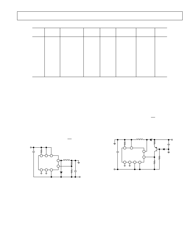
Figure 22. Positive-to-Negative Converter
The design criteria for the step-down application also apply to
the positive-to-negative converter. The output voltage should be
limited to |6.2 V| unless a diode is inserted in series with the
SW2 pin (see Figure 20.) Also, D1 must again be a Schottky
diode to prevent excessive power dissipation in the ADP1111.
NEGATIVE-TO-POSITIVE CONVERSION
The circuit of Figure 23 converts a negative input voltage to a
positive output voltage. Operation of this circuit configuration is
similar to the step-up topology of Figure 18, except the current
through feedback resistor R2 is level-shifted below ground by a
PNP transistor. The voltage across R2 is V
OUT
–V
BEQ1
. How-
ever, diode D2 level-shifts the base of Q1 about 0.6 V below
ground thereby cancelling the V
BE
of Q1. The addition of D2
also reduces the circuit’s output voltage sensitivity to tempera-
ture, which otherwise would be dominated by the –2 mV V
BE
contribution of Q1. The output voltage for this circuit is
determined by the formula:
V
OUT
=
1.25
V
R
2
R
1
Unlike the positive step-up converter, the negative-to-positive
converter’s output voltage can be either higher or lower than the
input voltage.
I
LIM
V
IN
SW1
SW2
4
FB
GND
5
SET
7
AO
6
ADP1111
NC
D1
1N5818
1
2
3
8
NC
C2
+
R1
10k
C
L
+
POSITIVE
OUTPUT
R2
MJE210
R
LIM
NEGATIVE
INPUT
L1
D2
2N3906
Q1
Figure 23. ADP1111 Negative-to-Positive Converter
LIMITING THE SWITCH CURRENT
The ADP1111’s R
LIM
pin permits the switch current to be
limited with a single resistor. This current limiting action occurs
on a pulse by pulse basis. This feature allows the input voltage
to vary over a wide range without saturating the inductor or
exceeding the maximum switch rating. For example, a particular
design may require peak switch current of 800 mA with a 2.0 V
input. If V
IN
rises to 4 V, however, the switch current will
exceed 1.6 A. The ADP1111 limits switch current to 1.5 A and
thereby protects the switch, but the output ripple will increase.
Selecting the proper resistor will limit the switch current to
800 mA, even if V
IN
increases. The relationship between R
LIM
and maximum switch current is shown in Figure 6.
The I
LIM
feature is also valuable for controlling inductor current
when the ADP1111 goes into continuous-conduction mode.
Table I. Component Selection for Typical Converters
Input
Voltage
Output
Voltage
Output
Current (mA)
Circuit
Figure
Inductor
Value
Inductor
Part No.
Capacitor
Value
Notes
2 to 3.1
2 to 3.1
2 to 3.1
2 to 3.1
5
5
6.5 to 11
12 to 20
20 to 30
5
12
5
5
12
12
12
12
5
5
5
–5
–5
90 mA
10 mA
30 mA
10 mA
90 MA
30 mA
50 mA
300 mA
300 mA
7 mA
250 mA
4
4
4
4
4
4
5
5
5
6
6
15
μ
H
47
μ
H
15
μ
H
47
μ
H
33
μ
H
47
μ
H
15
μ
H
56
μ
H
120
μ
H
56
μ
H
120
μ
H
CD75-150K
CTX50-1
CD75-150K
CTX50-1
CD75-330K
CTX50-1
33
μ
F
10
μ
F
22
μ
F
10
μ
F
22
μ
F
15
μ
F
47
μ
F
47
μ
F
47
μ
F
47
μ
F
100
μ
F
*
**
**
**
CTX50-4
CTX100-4
CTX50-4
CTX100-4
**
NOTES
CD = Sumida.
CTX = Coiltronics.
*
*Add 47
from I
LIM
to V
IN
.
**Add 220
from I
LIM
to V
IN
.
相關PDF資料 |
PDF描述 |
|---|---|
| ADP1111AN-12 | Micropower, Step-Up/Step-Down SW Regulator; Adjustable and Fixed 3.3 V, 5 V, 12 V |
| ADP1111AN-33 | Micropower, Step-Up/Step-Down SW Regulator; Adjustable and Fixed 3.3 V, 5 V, 12 V |
| ADP1111AN-5 | Micropower, Step-Up/Step-Down SW Regulator; Adjustable and Fixed 3.3 V, 5 V, 12 V |
| ADP1111 | Micropower, Step-Up/Step-Down Switching Regulator(微功耗,可調/固定輸出,步升/步降開關穩壓器) |
| ADP1147 | RADIATION HARDENED HIGH EFFICIENCY, 5 AMP SWITCHING REGULATORS |
相關代理商/技術參數 |
參數描述 |
|---|---|
| ADP1111AR-5 | 制造商:Analog Devices 功能描述:Conv DC-DC Single Non-Inv/Inv/Step Up/Step Down 2V to 30V 8-Pin SOIC N 制造商:Analog Devices 功能描述:IC SWITCHING REGULATOR |
| ADP1111AR-5-REEL | 制造商:Analog Devices 功能描述:Conv DC-DC Single Non-Inv/Inv/Step Up/Step Down 2V to 30V 8-Pin SOIC N T/R |
| ADP1111AR-REEL | 制造商:Analog Devices 功能描述: |
| ADP1111ARZ | 功能描述:IC REG BUCK BOOST INV ADJ 8SOIC RoHS:是 類別:集成電路 (IC) >> PMIC - 穩壓器 - DC DC 開關穩壓器 系列:- 標準包裝:250 系列:- 類型:降壓(降壓) 輸出類型:固定 輸出數:1 輸出電壓:1.2V 輸入電壓:2.05 V ~ 6 V PWM 型:電壓模式 頻率 - 開關:2MHz 電流 - 輸出:500mA 同步整流器:是 工作溫度:-40°C ~ 85°C 安裝類型:表面貼裝 封裝/外殼:6-UFDFN 包裝:帶卷 (TR) 供應商設備封裝:6-SON(1.45x1) 產品目錄頁面:1032 (CN2011-ZH PDF) 其它名稱:296-25628-2 |
| ADP1111ARZ-12 | 制造商:Analog Devices 功能描述:Conv DC-DC Single Non-Inv/Inv/Step Up/Step Down 2V to 30V 8-Pin SOIC N 制造商:Analog Devices 功能描述:V REG STEP UP/DOWN 12V SMD SOIC8 制造商:Analog Devices 功能描述:Switching Regulator 12V 0.2A SOIC8 |
發布緊急采購,3分鐘左右您將得到回復。