- 您現(xiàn)在的位置:買賣IC網(wǎng) > PDF目錄374018 > ADP1111AR (ANALOG DEVICES INC) Micropower, Step-Up/Step-Down SW Regulator; Adjustable and Fixed 3.3 V, 5 V, 12 V PDF資料下載
參數(shù)資料
| 型號(hào): | ADP1111AR |
| 廠商: | ANALOG DEVICES INC |
| 元件分類: | 穩(wěn)壓器 |
| 英文描述: | Micropower, Step-Up/Step-Down SW Regulator; Adjustable and Fixed 3.3 V, 5 V, 12 V |
| 中文描述: | 1.5 A SWITCHING REGULATOR, 88 kHz SWITCHING FREQ-MAX, PDSO8 |
| 封裝: | SOIC-8 |
| 文件頁(yè)數(shù): | 10/16頁(yè) |
| 文件大小: | 406K |
| 代理商: | ADP1111AR |
第1頁(yè)第2頁(yè)第3頁(yè)第4頁(yè)第5頁(yè)第6頁(yè)第7頁(yè)第8頁(yè)第9頁(yè)當(dāng)前第10頁(yè)第11頁(yè)第12頁(yè)第13頁(yè)第14頁(yè)第15頁(yè)第16頁(yè)
ADP1111
–10–
REV. 0
CIRCUIT OPERATION, STEP DOWN (BUCK) MODE)
The ADP1111’s step down mode is used to produce an output
voltage that is lower than the input voltage. For example, the
output of four NiCd cells (+4.8 V) can be converted to a +3 V
logic supply.
A typical configuration for step down operation of the ADP1111
is shown in Figure 19. In this case, the collector of the internal
power switch is connected to V
IN
and the emitter drives the
inductor. When the switch turns on, SW2 is pulled up towards
V
IN
. This forces a voltage across L1 equal to V
IN
– V
CE
– V
OUT
and causes current to flow in L1. This current reaches a final
value of:
I
PEAK
V
IN
V
CE
V
OUT
where 7
μ
s
is the ADP1111 switch’s “on” time.
L
7
μ
s
I
LIM
V
IN
SW1
SW2 4
GND
5
SET
7
AO
6
ADP1111
NC
L1
D1
1N5818
R
LIM
100
1
+
V
IN
2
3
NC
C
2
+
V
OUT
R2
R1
C
L
FB 8
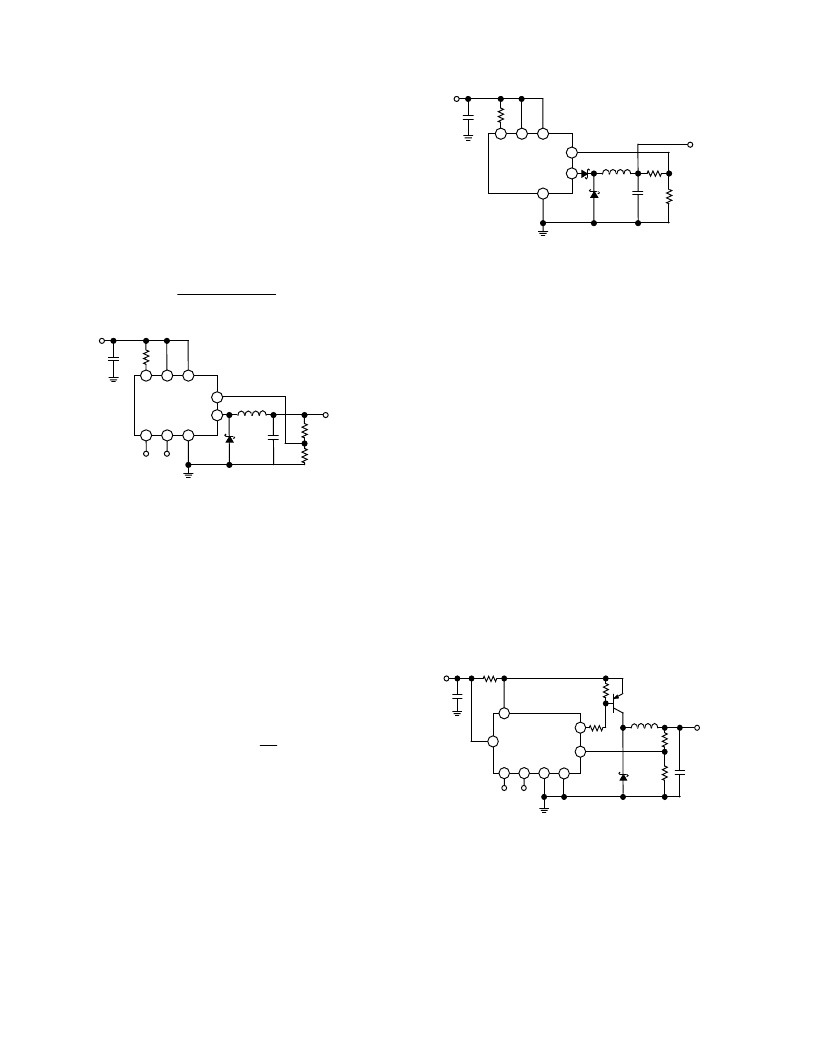
Figure 19. Step-Down Mode Operation
When the switch turns off, the magnetic field collapses. The
polarity across the inductor changes, and the switch side of the
inductor is driven below ground. Schottky diode D1 then turns
on, and current flows into the load. Notice that the Absolute
Maximum Rating for the ADP1111’s SW2 pin is 0.5 V below
ground. To avoid exceeding this limit, D1 must be a Schottky
diode. If a silicon diode is used for D1, Pin SW2 can go to
–0.8 V, which will cause potentially damaging power dissipation
within the ADP1111.
The output voltage of the buck regulator is fed back to the
ADP1111’s FB pin by resistors R1 and R2. When the voltage at
pin FB falls below 1.25 V, the internal power switch turns “on”
again, and the cycle repeats. The output voltage is set by the
formula:
V
OUT
=
1.25
V
1
+
R
2
R
1
When operating the ADP1111 in step-down mode, the output
voltage is impressed across the internal power switch’s emitter-
base junction when the switch is off. To protect the switch, the
output voltage should be limited to 6.2 V or less. If a higher
output voltage is required, a Schottky diode should be placed in
series with SW2 as shown in Figure 20.
I
LIM
V
IN
SW1
SW2
FB
GND
5
ADP1111
L1
D1
R
3
1
+
V
IN
2
3
8
4
C
2
+
V
OUT
R2
R1
D2
C
1
D1, D2 = 1N5818 SCHOTTKY DIODES
Figure 20. Step-Down Model, V
OUT
> 6.2 V
If the input voltage to the ADP1111 varies over a wide range, a
current limiting resistor at Pin 1 may be required. If a particular
circuit requires high peak inductor current with minimum input
supply voltage, the peak current may exceed the switch maxi-
mum rating and/or saturate the inductor when the supply
voltage is at the maximum value. See the “Limiting the Switch
Current” section of this data sheet for specific recommendations.
INCREASING OUTPUT CURRENT IN THE STEP-DOWN
REGULATOR
Unlike the boost configuration, the ADP1111’s internal power
switch is not saturated when operating in step-down mode. A
conservative value for the voltage across the switch in step-down
mode is 1.5 V. This results in high power dissipation within the
ADP1111 when high peak current is required. To increase the
output current, an external PNP switch can be added (Figure
21). In this circuit, the ADP1111 provides base drive to Q1
through R3, while R4 ensures that Q1 turns off rapidly. Because
the ADP1111’s internal current limiting function will not work
in this circuit, R5 is provided for this purpose. With the value
shown, R5 limits current to 2 A. In addition to reducing power
dissipation on the ADP1111, this circuit also reduces the switch
voltage. When selecting an inductor value for the circuit of
Figure 21, the switch voltage can be calculated from the
formula:
V
= V
+ V
0.6 V + 0.4 V
1 V
SW
R5
Q1(SAT)
I
LIM
V
IN
SW1
SW2
4
FB
GND
5
SET
7
AO
6
ADP1111
NC
L1
D1
1N5821
R5
0.3
1
INPUT
C
INPUT
+
2
3
8
NC
R1
R2
C
L
+
OUTPUT
R3
330
R4
220
Q1
MJE210
Figure 21. High Current Step-Down Operation
相關(guān)PDF資料 |
PDF描述 |
|---|---|
| ADP1111AN-3.3 | Micropower Step-Up/Step-Down SW Regulator. Adjustable and Fixed 3.3 V 5 V 12 V(406.88 k) |
| ADP1111AR-3.3 | Micropower Step-Up/Step-Down SW Regulator. Adjustable and Fixed 3.3 V 5 V 12 V(406.88 k) |
| ADP1111AN-12 | Micropower, Step-Up/Step-Down SW Regulator; Adjustable and Fixed 3.3 V, 5 V, 12 V |
| ADP1111AN-33 | Micropower, Step-Up/Step-Down SW Regulator; Adjustable and Fixed 3.3 V, 5 V, 12 V |
| ADP1111AN-5 | Micropower, Step-Up/Step-Down SW Regulator; Adjustable and Fixed 3.3 V, 5 V, 12 V |
相關(guān)代理商/技術(shù)參數(shù) |
參數(shù)描述 |
|---|---|
| ADP1111AR-12 | 制造商:Analog Devices 功能描述:Conv DC-DC Single Non-Inv/Inv/Step Up/Step Down 2V to 30V 8-Pin SOIC N 制造商:Rochester Electronics LLC 功能描述:MICROPOWER STEP-UP/DOWN SWITCHING REG. - Bulk |
| ADP1111AR-12-REEL | 制造商:Analog Devices 功能描述:Conv DC-DC Single Non-Inv/Inv/Step Up/Step Down 2V to 30V 8-Pin SOIC N T/R |
| ADP1111AR-3.3 | 制造商:Analog Devices 功能描述:Conv DC-DC Single Non-Inv/Inv/Step Up/Step Down 2V to 30V 8-Pin SOIC N 制造商:Rochester Electronics LLC 功能描述:MICROPOWER STEP-UP/DOWN SWITCHING REG. - Bulk |
| ADP1111AR-3.3-REEL | 制造商:Analog Devices 功能描述:Conv DC-DC Single Non-Inv/Inv/Step Up/Step Down 2V to 30V 8-Pin SOIC N T/R 制造商:Analog Devices 功能描述:CONV DC-DC SGL-OUT NON-INV/INV/STEP UP/STEP DOWN 8SOIC N - Tape and Reel |
| ADP1111AR-33 | 制造商:AD 制造商全稱:Analog Devices 功能描述:Micropower, Step-Up/Step-Down SW Regulator; Adjustable and Fixed 3.3 V, 5 V, 12 V |
發(fā)布緊急采購(gòu),3分鐘左右您將得到回復(fù)。