- 您現(xiàn)在的位置:買賣IC網(wǎng) > PDF目錄374019 > ADP3000AR-12 (ANALOG DEVICES INC) Top Entry Connector Hood; Enclosure Material:Aluminum Alloy; For Use With:C146 Rectangular Circular Connectors; Connecting Termination:Screw; Gender:Male; No. of Contacts:48; Operating Voltage:400V; Series:C-146 RoHS Compliant: Yes PDF資料下載
參數(shù)資料
| 型號(hào): | ADP3000AR-12 |
| 廠商: | ANALOG DEVICES INC |
| 元件分類: | 穩(wěn)壓器 |
| 英文描述: | Top Entry Connector Hood; Enclosure Material:Aluminum Alloy; For Use With:C146 Rectangular Circular Connectors; Connecting Termination:Screw; Gender:Male; No. of Contacts:48; Operating Voltage:400V; Series:C-146 RoHS Compliant: Yes |
| 中文描述: | SWITCHING REGULATOR, 400 kHz SWITCHING FREQ-MAX, PDSO8 |
| 封裝: | MS-012-AA, SOIC-8 |
| 文件頁數(shù): | 3/12頁 |
| 文件大小: | 342K |
| 代理商: | ADP3000AR-12 |
ADP3000
–3–
REV. 0
PIN DESCRIPTIONS
Mnemonic
I
LIM
Function
For normal conditions this pin is connected to
V
IN
. When lower current is required, a resistor
should be connected between I
LIM
and V
IN.
Limiting the switch current to 400 mA is
achieved by connecting a 220
resistor.
Input Voltage.
Collector of power transistor. For step-down
configuration, connect to V
IN.
For step-up
configuration, connect to an inductor/diode.
Emitter of power transistor. For step-down
configuration, connect to inductor/diode.
For step-up configuration, connect to ground.
Do not allow this pin to go more than a diode
drop below ground.
Ground.
Auxiliary Gain (GB) output. The open col-
lector can sink 300
μ
A. It can be left open
if not used.
SET Gain amplifier input. The amplifier’s
positive input is connected to SET pin and its
negative input is connected to 1.245 V. It can
be left open if not used.
On the ADP3000 (adjustable) version, this pin
is connected to the comparator input. On the
ADP3000-3.3, ADP3000-5 and ADP3000-12,
the pin goes directly to the internal resistor
divider that sets the output voltage.
V
IN
SW1
SW2
GND
AO
SET
FB/SENSE
WARNING!
ESD SENSITIVE DEVICE
CAUTION
ESD (electrostatic discharge) sensitive device. Electrostatic charges as high as 4000 V readily
accumulate on the human body and test equipment and can discharge without detection.
Although the ADP3000 features proprietary ESD protection circuitry, permanent damage may
occur on devices subjected to high energy electrostatic discharges. Therefore, proper ESD
precautions are recommended to avoid performance degradation or loss of functionality.
ABSOLUTE MAXIMUM RATINGS
Input Supply Voltage, Step-Up Mode . . . . . . . . . . . . . . . 15 V
Input Supply Voltage, Step-Down Mode . . . . . . . . . . . . . 36 V
SW1 Pin Voltage . . . . . . . . . . . . . . . . . . . . . . . . . . . . . . . 50 V
SW2 Pin Voltage . . . . . . . . . . . . . . . . . . . . . . . . –0.5 V to V
IN
Feedback Pin Voltage (ADP3000) . . . . . . . . . . . . . . . . . .5.5 V
Switch Current . . . . . . . . . . . . . . . . . . . . . . . . . . . . . . . .1.5 A
Maximum Power Dissipation . . . . . . . . . . . . . . . . . . 500 mW
Operating Temperature Range . . . . . . . . . . . . . 0
°
C to +70
°
C
Storage Temperature Range . . . . . . . . . . . . –65
°
C to +150
°
C
Lead Temperature (Soldering, 10 sec) . . . . . . . . . . . .+300
°
C
Thermal Impedance
SO-8 . . . . . . . . . . . . . . . . . . . . . . . . . . . . . . . . . . 170
°
C/W
N-8 . . . . . . . . . . . . . . . . . . . . . . . . . . . . . . . . . . . 120
°
C/W
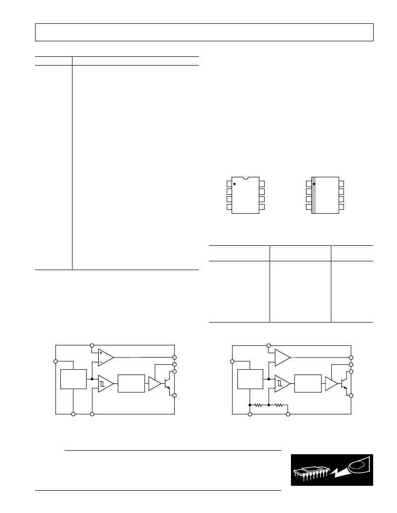
PIN CONFIGURATIONS
8-Lead Plastic DIP 8-Lead SOIC
(N-8) (SO-8)
1
2
3
4
8
7
6
5
TOP VIEW
(Not to Scale)
ADP3000
I
LIM
V
IN
SW1
SW2
FB (SENSE)*
SET
AO
GND
* FIXED VERSIONS
1
2
3
4
8
7
6
5
(TOP VIEW
ADP3000
I
LIM
V
IN
SW1
SW2
FB (SENSE)*
SET
AO
GND
* FIXED VERSIONS
ORDERING GUIDE
Output
Voltage
3.3 V
3.3 V
5 V
5 V
12 V
12 V
Adjustable
Adjustable
Package
Option
N-8
SO-8
N-8
SO-8
N-8
SO-8
N-8
SO-8
Model
ADP3000AN-3.3
ADP3000AR-3.3
ADP3000AN-5
ADP3000AR-5
ADP3000AN-12
ADP3000AR-12
ADP3000AN
ADP3000AR
N = plastic DIP, SO = small outline package.
Figure 3a. Functional Block Diagram for Adjustable Version
Figure 3b. Functional Block Diagram for Fixed Version
COMPARATOR
GAIN BLOCK/
ERROR AMP
OSCILLATOR
DRIVER
A2
1.245V
REFERENCE
ADP3000
SET
V
IN
GND
FB
A0
I
LIM
SW1
SW2
A1
COMPARATOR
GAIN BLOCK/
ERROR AMP
OSCILLATOR
DRIVER
A1
1.245V
REFERENCE
R1
R2
ADP3000
SET
V
IN
GND
SENSE
A0
I
LIM
SW1
SW2
相關(guān)PDF資料 |
PDF描述 |
|---|---|
| ADP3025JRU-REEL | High Efficiency Dual Output Power Supply Controller |
| ADP3025 | High Efficiency Dual Output Power Supply Controller |
| ADP3050AR-33 | Circular Connector Cable Assembly; Connector Type A:Circular Plug; Connector Type B:Stripped End Leads; Cable Length:10ft RoHS Compliant: Yes |
| ADP3050AR-5 | Circular Connector Cable Assembly; Connector Type A:Circular Receptacle; Connector Type B:Stripped End Leads; Cable Length:10ft RoHS Compliant: Yes |
| ADP3050 | 200 kHz, 1 A High-Voltage Step-Down Switching Regulator |
相關(guān)代理商/技術(shù)參數(shù) |
參數(shù)描述 |
|---|---|
| ADP3000AR-12-REEL | 制造商:Analog Devices 功能描述: |
| ADP3000AR-3.3 | 制造商:Rochester Electronics LLC 功能描述:MCROPWR STPUP/DWN H. FRQ. SWT. REG. 3.3V - Bulk |
| ADP3000AR-3.3-REEL | 制造商:Rochester Electronics LLC 功能描述:- Tape and Reel |
| ADP3000AR-33 | 制造商:AD 制造商全稱:Analog Devices 功能描述:Micropower Step-Up/Step-Down Fixed 3.3 V, 5 V, 12 V and Adjustable High Frequency Switching Regulator |
| ADP3000AR-5 | 制造商:Analog Devices 功能描述:Conv DC-DC Single Non-Inv/Inv/Step Up/Step Down 2V to 30V 8-Pin SOIC N |
發(fā)布緊急采購,3分鐘左右您將得到回復(fù)。