- 您現在的位置:買賣IC網 > PDF目錄374019 > ADP3156 (Analog Devices, Inc.) Dual Power Supply Controller for Desktop Systems PDF資料下載
參數資料
| 型號: | ADP3156 |
| 廠商: | Analog Devices, Inc. |
| 英文描述: | Dual Power Supply Controller for Desktop Systems |
| 中文描述: | 雙電源控制器桌面系統 |
| 文件頁數: | 7/12頁 |
| 文件大小: | 186K |
| 代理商: | ADP3156 |
REV. 0
ADP3156
–7–
During the standby operating state, the 12 V, 5 V and 3.3 V
power supply outputs are disabled, and only a low power 5 V
rail (5VSB) is available. The circuits that must remain active in
standby must be able to run from 5VSB. To accomplish this,
power routing is required to allow switching between normal
and standby supplies. Lack of a 12 V rail in standby makes control
of linear outputs difficult, and with up to 8 A demand from the
1.5 V and 1.8 V rails, an all-linear solution is inefficient.
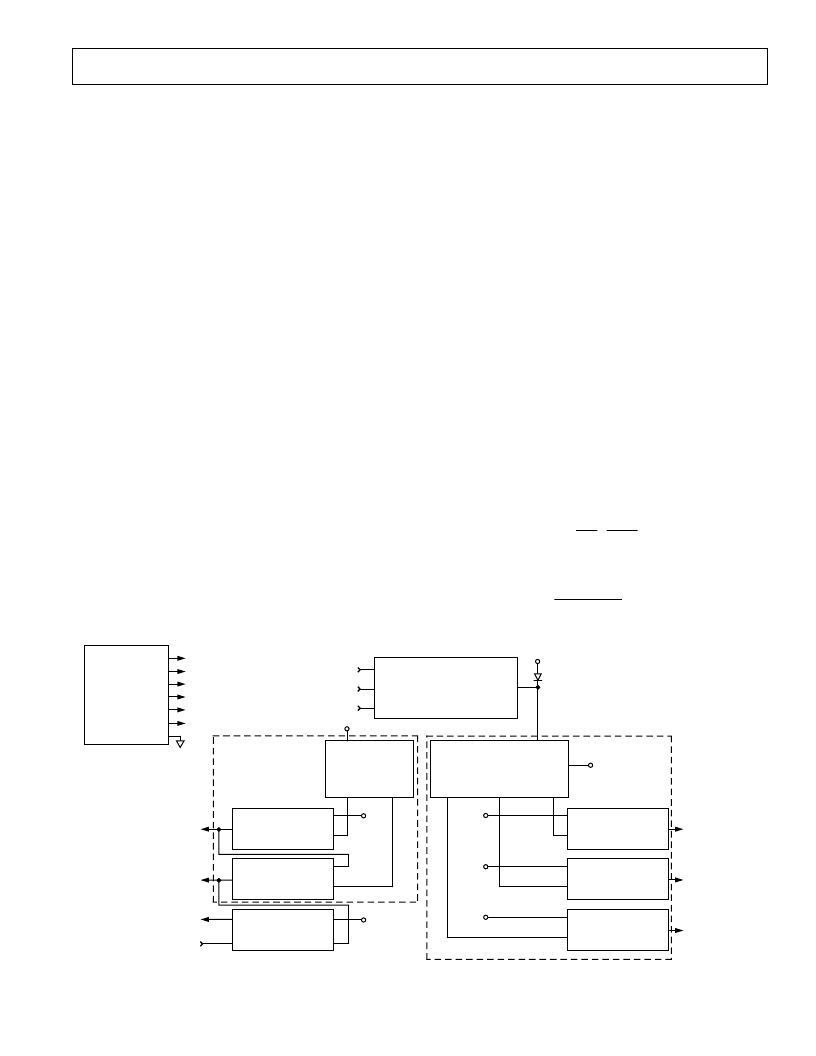
Figure 13 shows a typical ACP-compliant Pentium III / chipset
power management system using the ADP3155 and ADP3156.
The ADP3155 provides VID switched output and two linear
regulators for standby operation. A charge-pump-doubled 5VSB is
ORed into the supply rail to supply the linear regulators during
standby operation. The VID output collapses when the main
5 V rail collapses, but the N-channel MOSFET linear regu-
lators can continue to supply current from the ~9 V supply.
The ADP3156 provides 1.8 V via its main switching regulator,
and allows efficient linear regulation of 1.5 V rail by using the
1.8 V output as its source.
The design parameters for an ACPI-compliant Pentium III
peripheral system depend on what peripherals are used
(e.g., AGP) and what their specifications are. The following is
an example where the higher of two low system voltages (1.8 V
and 1.5 V) is created directly with the main buck converter, and
also used to supply power for the lower output voltage using the
ADP3156’s linear regulator controller.
Input voltage (power source): V
IN
= 5 V
Auxiliary voltage: V
CC
= 12 V
Output voltages and tolerances: V
1
= 1.8 V
±
5%, V
2
= 1.5 V
±
5%
Maximum output currents: I
1MAX
= 3 A, I
2MAX
= 4 A
Slew rate of load current change: di
1
/dt = di
2
/dt >10 A/
μ
s
The absence of an inductor on the 1.5 V linear regulated output
allows the output current to respond quickly and the linear
regulator MOSFET’s resistance to be modulated quickly. This,
and some small bypassing capacitors, essentially insulates the
1.5 V output from transient activity on the 1.8 V output. How-
ever, this same fast response characteristic means that any 1.5V
transient activity will be passed straight through the linear regu-
lator to the 1.8 V output. This means that the 1.8 V output filter
capacitor selection must consider both 1.8 V and 1.5 V load
transients.
In this design example, worst case consideration requires that
the 1.8 V output be designed for transient current loading of
I
1MAX
+ I
2MAX
= 7 A. Also, because a practical switching regula-
tor design will have a current slew rate of <1 A/
μ
s due to the
inductor, nearly the entire 7 A transient current must be ab-
sorbed by the output capacitors.
C
T
Selection for Operating Frequency
The ADP3156 uses a constant-off-time architecture with t
OFF
determined by an external timing capacitor C
T
. Each time the
high side N-channel MOSFET switch turns on, the voltage
across C
T
is reset to approximately 3.3 V. During the off-time,
C
T
is discharged by a constant current of 65
μ
A. Once C
T
reaches
2.3 V, a new on-time cycle is initiated. The value of the off-time
is calculated using the continuous-mode operating frequency.
Assuming a nominal operating frequency of f
NOM
= 200 kHz at
an output voltage of 1.8 V, the corresponding off-time is:
t
V
V
f
s
OFF
O
IN
NOM
=
=
1
1
3 2
.
–
μ
The timing capacitor can be calculated from the equation:
C
t
A
V
pF
T
OFF
=
×
1
=
65
208
μ
5V_PM
POWER
MANAGEMENT
FUNCTIONS
V
CC
12V
POWER MANAGEMENT
STATE COMMAND
5V_PM
ATX_POWER GOOD
PMSC
5V_PM
ATXPG
V
CC
ADP3155
VID_4:0
LIN#2_
CTRLS
LIN#1_
CTRLS
MAIN_
CTRLS
SWITCHER
CTRLS
IN
OUT
LINEAR#1
CTRLS
IN
OUT
LINEAR#2
IN
CTRLS
OUT
5V
5V_PM
CPU
V
CORE
@ VID
3.3V_PM
FOR POWER
MANAGEMENT
TRIPLE
OUTPUT
SUPPLY
VID
V
CC
ADP3156
LIN_
CTRLS
MAIN_
CTRLS
12V
DUAL
OUTPUT
SUPPLY
IN
CTRLS
OUT
SWITCHER
5V
IN
CTRLS
OUT
LINEAR
3.3V_IN
1.5V_IN
VDDQ
POWER ROUTING
SELECT
3.3V
1.8V FOR
SB CORE,
MEM, ETC
1.5V VTT
FOR GTL
1.5V OR 3.3V
VDDQ FOR AGP
TYPEDET# FOR
AGP SELECT
ATX
(OR NLX)
POWER
SUPPLY
12V
5V
3.3V
5V_ALWAYS
ATX_PGOOD
ATX_SHUTDOWN
GND
12V
5V
3.3V
5V_PM
ATX_POWERGOOD
ATX_SHUTDOWN
2.5V_PM
FOR CMOS,
CLOCK, MEMORY
Figure 13. ACPI-Compliant Pentium III System Block Diagram
相關PDF資料 |
PDF描述 |
|---|---|
| ADP3160 | 5-Bit Programmable 2-Phase Synchronous Buck Controller |
| ADP3160JR | 5-Bit Programmable 2-Phase Synchronous Buck Controller |
| ADP3167JR | 5-Bit Programmable 2-Phase Synchronous Buck Controller |
| ADP3163JRU | 5-Bit Programmable 2-/3-Phase Synchronous Buck Controller |
| ADP3163 | 500-mA, 4.2-V Li-Ion Charger for Current-Limited App. w/Temp Sense in MSOP-8 8-MSOP-PowerPAD -40 to 85 |
相關代理商/技術參數 |
參數描述 |
|---|---|
| ADP3156JR-1.5 | 制造商:Rochester Electronics LLC 功能描述:- Bulk |
| ADP3156JR-1.5-REEL | 制造商:Rochester Electronics LLC 功能描述:- Tape and Reel |
| ADP3156JR-1.8 | 制造商:Rochester Electronics LLC 功能描述:- Bulk |
| ADP3156JR-1.8-REEL | 制造商:Rochester Electronics LLC 功能描述:- Tape and Reel |
| ADP3156JR-15 | 制造商:AD 制造商全稱:Analog Devices 功能描述:Dual Power Supply Controller for Desktop Systems |
發布緊急采購,3分鐘左右您將得到回復。