- 您現(xiàn)在的位置:買賣IC網(wǎng) > PDF目錄374019 > ADP3156JR-15 (Analog Devices, Inc.) Dual Power Supply Controller for Desktop Systems PDF資料下載
參數(shù)資料
| 型號: | ADP3156JR-15 |
| 廠商: | Analog Devices, Inc. |
| 英文描述: | Dual Power Supply Controller for Desktop Systems |
| 中文描述: | 雙電源控制器桌面系統(tǒng) |
| 文件頁數(shù): | 3/12頁 |
| 文件大小: | 186K |
| 代理商: | ADP3156JR-15 |
REV. 0
ADP3156
–3–
ABSOLUTE MAXIMUM RATINGS*
Input Supply Voltage (V
CC
) . . . . . . . . . . . . . . .–0.3 V to +16 V
Shutdown Input Voltage . . . . . . . . . . . . . . . . –0.3 V to +16 V
Operating Ambient Temperature Range . . . . . . 0
°
C to +70
°
C
Junction Temperature Range . . . . . . . . . . . . . . 0
°
C to +150
°
C
θ
JA
. . . . . . . . . . . . . . . . . . . . . . . . . . . . . . . . . . . . . 90
°
C/W
Storage Temperature Range . . . . . . . . . . . . –65
°
C to +150
°
C
Lead Temperature (Soldering, 10 sec) . . . . . . . . . . . +300
°
C
*This is a stress rating only; operation beyond these limits can cause the device to
be permanently damaged.
ORDERING GUIDE
Buck Converter
Output Voltage
Package
Option
Model
ADP3156JR-1.5
ADP3156JR-1.8
ADP3156JR-2.5
1.5 V
1.8 V
2.5 V
R-16A/SO-16
R-16A/SO-16
R-16A/SO-16
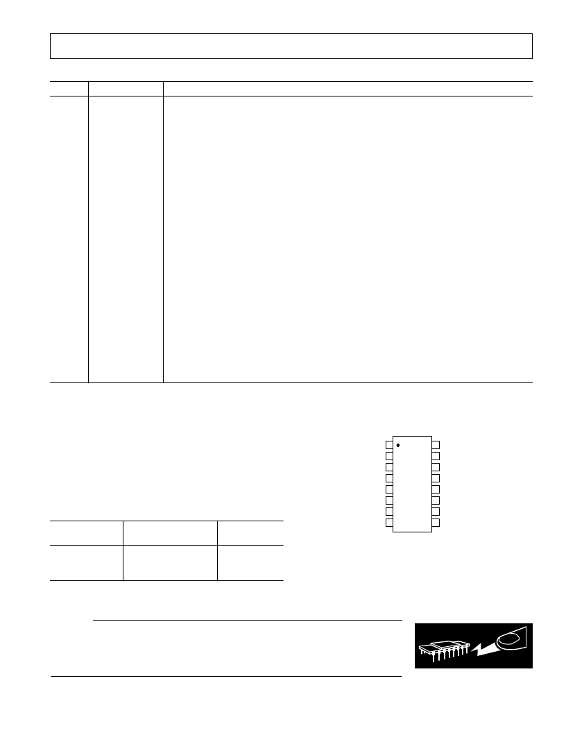
PIN CONFIGURATION
16-Lead SOIC
TOP VIEW
(Not to Scale)
16
15
14
13
12
11
10
9
1
2
3
4
5
6
7
8
NC = NO CONNECT
NC
NC
AGND
SD
FB
V
LDO
SENSE–
SENSE+
PGND
NC
DRIVE1
DRIVE2
V
CC
PWRGD
CMP
C
T
ADP3156
PIN FUNCTION DESCRIPTIONS
Pin
Mnemonic
Function
1, 2, 15
3
4
NC
AGND
SD
No Connect.
Analog Ground. All internal signals of the ADP3156 are referenced to this ground.
Shutdown. A logic high will place the ADP3156 in shutdown and disable both outputs. This pin
is internally pulled down.
Feedback connection for the linear controller. Connect this pin to the resistor divider network to
set the output voltage of the linear regulator.
Gate Drive for the linear regulator N-channel MOSFET.
Connects to the internal resistor divider that senses the output voltage. This pin is also the refer-
ence input for the current comparator.
(+) input for the current comparator. The output current is sensed as a voltage at this pin with
respect to SENSE–.
External Capacitor C
T
connection to ground sets the off-time of the device.
Error Amplifier output and compensation point. The voltage at this output programs the
output current control level between the SENSE pins.
Power Good. An open drain signal indicates the output voltage is within a
±
5% regulation band.
Supply Voltage to ADP3156.
Gate Drive for the (bottom) Synchronous Rectifier N-channel MOSFET. The voltage at DRIVE2
swings from ground to V
CC
.
Gate Drive for the buck switch N-channel MOSFET. The voltage at DRIVE1 swings from
ground to V
CC
.
Power Ground. The drivers turn off the buck and synchronous MOSFETs by discharging their
gate capacitances to this pin. PGND should have a low impedance path to the source of the syn-
chronous MOSFET.
5
FB
6
7
V
LDO
SENSE–
8
SENSE+
9
10
C
T
CMP
11
12
13
PWRGD
V
CC
DRIVE2
14
DRIVE1
16
PGND
CAUTION
ESD (electrostatic discharge) sensitive device. Electrostatic charges as high as 4000 V readily
accumulate on the human body and test equipment and can discharge without detection.
Although the ADP3156 features proprietary ESD protection circuitry, permanent damage may
occur on devices subjected to high energy electrostatic discharges. Therefore, proper ESD
precautions are recommended to avoid performance degradation or loss of functionality.
WARNING!
ESD SENSITIVE DEVICE
相關(guān)PDF資料 |
PDF描述 |
|---|---|
| ADP3156JR-18 | Dual Power Supply Controller for Desktop Systems |
| ADP3156JR-25 | Dual Power Supply Controller for Desktop Systems |
| ADP3156 | Dual Power Supply Controller for Desktop Systems |
| ADP3160 | 5-Bit Programmable 2-Phase Synchronous Buck Controller |
| ADP3160JR | 5-Bit Programmable 2-Phase Synchronous Buck Controller |
相關(guān)代理商/技術(shù)參數(shù) |
參數(shù)描述 |
|---|---|
| ADP3156JR-18 | 制造商:AD 制造商全稱:Analog Devices 功能描述:Dual Power Supply Controller for Desktop Systems |
| ADP3156JR-2.5 | 制造商:Rochester Electronics LLC 功能描述:- Bulk |
| ADP3156JR-25 | 制造商:AD 制造商全稱:Analog Devices 功能描述:Dual Power Supply Controller for Desktop Systems |
| ADP3157 | 制造商:AD 制造商全稱:Analog Devices 功能描述:5-Bit Programmable Synchronous Controller for Pentium III Processors |
| ADP3157J | 制造商:Analog Devices 功能描述: |
發(fā)布緊急采購,3分鐘左右您將得到回復(fù)。