- 您現在的位置:買賣IC網 > PDF目錄374020 > ADP3171JR (ANALOG DEVICES INC) Charger front end protection IC with 30V max Vin and 4.5V LDO output 8-WSON 0 to 125 PDF資料下載
參數資料
| 型號: | ADP3171JR |
| 廠商: | ANALOG DEVICES INC |
| 元件分類: | 穩壓器 |
| 英文描述: | Charger front end protection IC with 30V max Vin and 4.5V LDO output 8-WSON 0 to 125 |
| 中文描述: | SWITCHING CONTROLLER, PDSO14 |
| 封裝: | SOIC-14 |
| 文件頁數: | 6/12頁 |
| 文件大小: | 310K |
| 代理商: | ADP3171JR |
REV. 0
–6–
ADP3171
Pentium is a registered trademark of Intel Corporation.
be disabled in standby mode, but the linear regulators will
begin
conducting once VCC rises above about 1 V. During
startup, the
linear outputs will track the 3.3 V supply up until
they reach their
respective regulation points, regardless of the
state of the 12 V supply. Once the 12 V supply has exceeded
the 5 VSB supply, the controller IC will track the 12 V supply.
Once the 12 V supply has risen above the UVLO value, the
switching regulator will begin its start-up sequence.
APPLICATION INFORMATION
Specifications for a Design Example
The design parameters for a typical auxiliary supply for a Pen-
tium III application (shown in Figure 3) are as follows:
Input Voltage: (V
IN
) = 5 V
Auxiliary Input: (V
CC
) = 12 V
Main Output: (V
OUT
) = 1.5 V @ 5 A
LDO 1 Output: (1.5 VSB) = 1.5 V @ 35 mA
LDO 2 Output: (3.3 VSB) = 3.3 V @ 1.5 A
CT Selection for Operating Frequency
The ADP3171 uses a constant off time architecture, with t
OFF
determined by an external timing capacitor CT. Each time the
high side N-channel MOSFET switch turns on, the voltage across
CT is reset to approximately 0 V. During the off time, CT is
charged by a constant current of 150
μ
A. Once CT reaches 3.0 V,
a new on time cycle is initiated. The value of the off time is
calculated using the continuous-mode operating frequency.
Assuming a nominal operating frequency (f
NOM
) of 200 kHz at
an output voltage of 1.5 V, the corresponding off time is:
t
V
V
f
t
V
V
kHz
s
OFF
OUT
IN
NOM
OFF
=
×
×
=
=
1
1
1
1 5
5
1
200
3 5
.
μ
–
–
.
(1)
The timing capacitor can be calculated from the equation:
C
t
I
V
A
V
pF
T
OFF
CT
T(TH)
=
×
=
×
3
=
3 5
.
μ
150
175
μ
s
(2)
f
t
V
I
R
R
R
–
V
V
I
–
–
R
m
m
R
+
R
1 5
28
R
f
s
V
V
A
A
m
m
m
m
V
MIN
OFF
IN
–
O MAX
(
DS ON HSF
(
SENSE
L
OUT
IN
5
5
O MAX
5
5
DS ON HSF
+
+
7 5
SENSE
3
3
L
DS ON LSF
(
MIN
=
×
×
+
+
×
15
15
(
+
+
+
)– .
–
=
×
×
×
1
1
3 5
.
7 5
.
.
–
(
)–
(
)
(
)
)
(
)
(
)
)
μ
=
192
m
kHz
)
(3)
The nearest standard value is 150 pF. The converter operates at
the nominal operating frequency only at the above specified V
OUT
and at light load. At higher values of V
OUT
, or under heavy load,
the operating frequency decreases due to the parasitic voltage
drops across the power devices. The actual
minimum frequency
at V
OUT
= 1.5 V is calculated to be 192 kHz
(see Equation 3),
where:
R
DS(ON)HSF
is the resistance of the high side MOSFET
(estimated value: 15 m
)
R
DS(ON)LSF
is the resistance of the low side MOSFET
(estimated value: 28 m
)
R
SENSE
is the resistance of the sense resistor
(estimated value: 7.5 m
)
R
L
is the resistance of the inductor (estimated value: 3 m
)
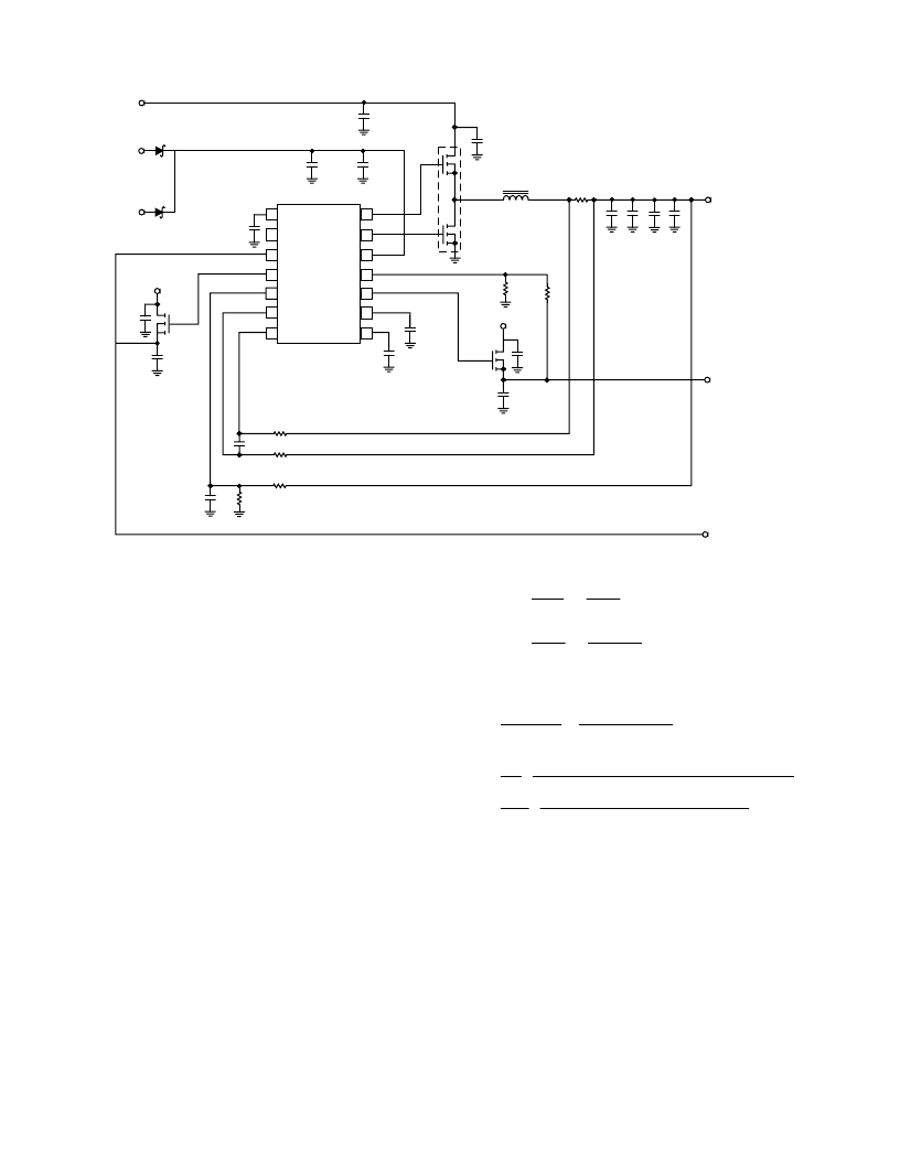
Figure 3. Pentium
III Auxiliary Supply Generating 1.5 V, 1.5 V Standby, and 3.3 V Standby
5VSB
12V
D2
MBR052LT1
+C6
4.7 F
C7
100nF
5V
D1
MBR052LT1
+C5
1000 F
GND
PWRGD
LRFB1
FB
CS–
CS+
LRDRV1
DRVH
DRVL
VCC
LRFB2
LRDRV2
COMP
CT
1
2
3
4
5
6
7
8
9
10
11
12
13
14
C8
22 F
L1
1.7 H
Q2
FDS6982
R6
7.5m
820 F 4
7.5m
ESR (EACH)
C14 C15 C16 C17
1.5V, 5A
3.3VSB, 1.5A
1.5VSB, 35mA
R4
249
R2
220
R1
220
C3
1nF
C3
100pF
R3
1k
C2
10 F
C1
1 F
Q1
2N7000
5VSB
R9
8.25k
R8
10k
5VSB
C12
1 F
C13
220 F
C10
100pF
C9
150pF
Q3
IRFU014
+
相關PDF資料 |
PDF描述 |
|---|---|
| ADP3171 | Charger front end protection IC with 30V max Vin and 4.5V LDO output 8-WSON 0 to 125 |
| ADP3179 | 4-Bit Programmable Synchronous Buck Controllers |
| ADP3179JRU | PRECISION THERMOSTATS |
| ADP3180JRU-REEL | Aluminum Electrolytic Radial Leaded Bi-Polar Capacitor; Capacitance: 470uF; Voltage: 35V; Case Size: 12.5x25 mm; Packaging: Bulk |
| ADP3180 | 6-Bit Programmable 2-, 3-, 4-Phase Synchronous Buck Controller |
相關代理商/技術參數 |
參數描述 |
|---|---|
| ADP3171JR-REEL7 | 制造商:Rochester Electronics LLC 功能描述:1.2V VTT BUCK CNTRLR W/2 LDOS & PWR GOOD - Tape and Reel |
| ADP3178 | 制造商:AD 制造商全稱:Analog Devices 功能描述:4-Bit Programmable Synchronous Buck Controllers |
| ADP3178JR | 制造商:Rochester Electronics LLC 功能描述:- Bulk |
| ADP3178JRZ-REEL7 | 功能描述:IC REG BUCK 4BIT ADJ VLT 16-SOIC RoHS:是 類別:集成電路 (IC) >> PMIC - 穩壓器 - 專用型 系列:- 標準包裝:2,000 系列:- 應用:控制器,DSP 輸入電壓:4.5 V ~ 25 V 輸出數:2 輸出電壓:最低可調至 1.2V 工作溫度:-40°C ~ 85°C 安裝類型:表面貼裝 封裝/外殼:30-TFSOP(0.173",4.40mm 寬) 供應商設備封裝:30-TSSOP 包裝:帶卷 (TR) |
| ADP3179 | 制造商:AD 制造商全稱:Analog Devices 功能描述:4-Bit Programmable Synchronous Buck Controllers |
發布緊急采購,3分鐘左右您將得到回復。