- 您現在的位置:買賣IC網 > PDF目錄374022 > ADP3339 (Analog Devices, Inc.) Cap-Free, NMOS, 150mA Low Dropout Regulator with Reverse Current Protection PDF資料下載
參數資料
| 型號: | ADP3339 |
| 廠商: | Analog Devices, Inc. |
| 元件分類: | 基準電壓源/電流源 |
| 英文描述: | Cap-Free, NMOS, 150mA Low Dropout Regulator with Reverse Current Protection |
| 中文描述: | 無電容,NMOS管,150mA的低壓差穩壓器的反向電流保護 |
| 文件頁數: | 6/8頁 |
| 文件大小: | 209K |
| 代理商: | ADP3339 |
REV. 0
ADP3339
–6–
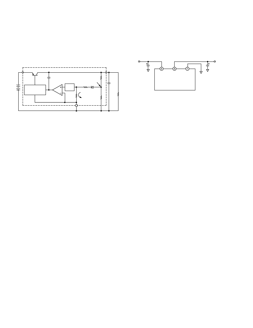
THEORY OF OPERATION
The new anyCAP
LDO ADP3339 uses a single control loop for
regulation and reference functions. The output voltage is sensed
by a resistive voltage divider consisting of R1 and R2 which is
varied to provide the available output voltage option. Feedback
is taken from this network by way of a series diode (D1) and a
second resistor divider (R3 and R4) to the input of an amplifier.
PTAT
V
OS
g
m
NONINVERTING
WIDEBAND
DRIVER
INPUT
Q1
ADP3339
COMPENSATION
CAPACITOR
ATTENUATION
(V
BANDGAP
/V
OUT
)
R3
R1
D1
R2
R4
OUTPUT
PTAT
CURRENT
(a)
GND
C
LOAD
R
LOAD
Figure 2. Functional Block Diagram
A very high-gain error amplifier is used to control this loop. The
amplifier is constructed in such a way that equilibrium pro-
duces a large, temperature-proportional input, “offset voltage”
that is repeatable and very well controlled. The temperature-
proportional offset voltage is combined with the complementary
diode voltage to form a “virtual bandgap” voltage, implicit in
the network, although it never appears explicitly in the circuit.
Ultimately, this patented design makes it possible to control
the loop with only one amplifier. This technique also improves
the noise characteristics of the amplifier by providing more flexibil-
ity on the trade-off of noise sources that leads to a low noise design.
The R1, R2 divider is chosen in the same ratio as the bandgap
voltage to the output voltage. Although the R1, R2 resistor divider
is loaded by the diode D1 and a second divider consisting of R3
and R4, the values can be chosen to produce a temperature-stable
output. This unique arrangement specifically corrects for the load-
ing of the divider, thus avoiding the error resulting from base
current loading in conventional circuits.
The patented amplifier controls a new and unique noninverting
driver that drives the pass transistor, Q1. The use of this special
noninverting driver enables the frequency compensation to
include the load capacitor in a pole-splitting arrangement to
achieve reduced sensitivity to the value, type, and ESR of the
load capacitance.
Most LDOs place very strict requirements on the range of ESR
values for the output capacitor because they are difficult to stabilize
due to the uncertainty of load capacitance and resistance. More-
over, the ESR value, required to keep conventional LDOs stable,
changes depending on load and temperature. These ESR limita-
tions make designing with LDOs more difficult because of their
unclear specifications and extreme variations over temperature.
With the ADP3339 anyCAP LDO, this is no longer true. It
can be used with virtually any good quality capacitor, with no
constraint on the minimum ESR. This innovative design allows
the circuit to be stable with just a small 1
μ
F capacitor on the out-
put. Additional advantages of the pole-splitting scheme include
superior line noise rejection and very high regulator gain, which
leads to excellent line and load regulation. An impressive
±
1.5
accuracy is guaranteed over line, load, and temperature.
Additional features of the circuit include current limit and ther-
mal shutdown.
V
IN
OUT
ADP3339
C1
1 F
C2
1 F
V
OUT
GND
IN
Figure 3. Typical Application Circuit
A
PPLICATION INFORMATION
CAPACITOR SELECTION
Output Capacitor
The stability and transient response of the LDO is a function of
the output capacitor. The ADP3339 is stable with a wide range
of capacitor values, types, and ESR (anyCAP). A capacitor as
low as 1
μ
F is all that is needed for stability. A higher capacitance
may be necessary if high output current surges are anticipated or
if the output capacitor cannot be located near the output and
ground pins. The ADP3339 is stable with extremely low ESR
capacitors (ESR 0), such as Multilayer Ceramic Capacitors
(MLCC) or OSCON. Note that the effective capacitance of
some capacitor types fall below the minimum over temperature
or with dc voltage.
Input Capacitor
An input bypass capacitor is not strictly required but it is recom-
mended in any application involving long input wires or high
source impedance. Connecting a 1
μ
F capacitor from the
input to ground reduces the circuit’s sensitivity to PC board
layout and input transients. If a larger output capacitor is neces-
sary, then a larger value input capacitor is also recommended.
OUTPUT CURRENT LIMIT
The ADP3339 is short-circuit protected by limiting the pass
transistor’s base drive current. The maximum output current is
limited to about 3 A, see TPC 13.
THERMAL OVERLOAD PROTECTION
The ADP3339 is protected against damage due to excessive power
dissipation by its thermal overload protection circuit. Thermal
protection limits the die temperature to a maximum of 160
°
C.
Under extreme conditions (i.e., high ambient temperature and
power dissipation) where the die temperature starts to rise above
160
°
C, the output current will be reduced until the die tempera-
ture has dropped to a safe level.
Current and thermal limit protections are intended to protect
the device against accidental overload conditions. For normal
operation, the device’s power dissipation should be externally
limited so that the junction temperature will not exceed 125
°
C.
相關PDF資料 |
PDF描述 |
|---|---|
| ADP3339AKC-25 | Circular Connector; No. of Contacts:85; Series:MS27474; Body Material:Aluminum; Connecting Termination:Crimp; Connector Shell Size:22; Circular Contact Gender:Pin; Circular Shell Style:Jam Nut Receptacle; Insert Arrangement:22-2 RoHS Compliant: No |
| ADP3339AKC-285 | JT 100C 100#22D SKT RECP |
| ADP3339AKC-33 | Circular Connector; No. of Contacts:55; Series:MS27474; Body Material:Aluminum; Connecting Termination:Crimp; Connector Shell Size:22; Circular Contact Gender:Socket; Circular Shell Style:Jam Nut Receptacle; Insert Arrangement:22-55 RoHS Compliant: No |
| ADP3339AKC-5 | Circular Connector; No. of Contacts:24; Series:MS27474; Body Material:Aluminum; Connecting Termination:Crimp; Connector Shell Size:24; Circular Contact Gender:Pin; Circular Shell Style:Jam Nut Receptacle; Insert Arrangement:24-24 RoHS Compliant: No |
| ADP3367* | +5 V Fixed. Adjustable Low-Dropout Linear Voltage Regulator |
相關代理商/技術參數 |
參數描述 |
|---|---|
| ADP3339AKC-1.5-RL | 制造商:Analog Devices 功能描述:REG LDO LIN FIX POS 1.5V 2A 4PIN SOT-223 - Tape and Reel |
| ADP3339AKC-1.5-RL7 | 功能描述:IC REG LDO 1.5V 1.5A SOT-223 RoHS:否 類別:集成電路 (IC) >> PMIC - 穩壓器 - 線性 系列:anyCAP® 標準包裝:3,000 系列:- 穩壓器拓撲結構:正,固定式和可調式 輸出電壓:3.3V,1.25 V ~ 5.7 V 輸入電壓:4.5 V ~ 7 V 電壓 - 壓降(標準):1.1V @ 1A 穩壓器數量:2 電流 - 輸出:1A 電流 - 限制(最小):1A 工作溫度:0°C ~ 125°C 安裝類型:表面貼裝 封裝/外殼:TO-252-5,DPak(4 引線 + 接片),TO-252AD 供應商設備封裝:PPAK 包裝:管件 其它名稱:497-3576-5 |
| ADP3339AKC-1.8 | 制造商:未知廠家 制造商全稱:未知廠家 功能描述:Analog IC |
| ADP3339AKC-1.8-RL | 制造商:Analog Devices 功能描述:LDO Regulator Pos 1.8V 2A 4-Pin(3+Tab) SOT-223 T/R |
| ADP3339AKC-1.8-RL7 | 制造商:Analog Devices 功能描述:LDO Regulator Pos 1.8V 2A 4-Pin(3+Tab) SOT-223 T/R 制造商:Rochester Electronics LLC 功能描述:1.5A ANYCAP LDO - Tape and Reel |
發布緊急采購,3分鐘左右您將得到回復。