- 您現(xiàn)在的位置:買賣IC網(wǎng) > PDF目錄374022 > ADP3410KRU (ANALOG DEVICES INC) Dual MOSFET Driver with Bootstrapping PDF資料下載
參數(shù)資料
| 型號(hào): | ADP3410KRU |
| 廠商: | ANALOG DEVICES INC |
| 元件分類: | MOSFETs |
| 英文描述: | Dual MOSFET Driver with Bootstrapping |
| 中文描述: | 2 CHANNEL, HALF BRDG BASED MOSFET DRIVER, PDSO14 |
| 封裝: | MO-153AB-1, TSSOP-14 |
| 文件頁(yè)數(shù): | 4/11頁(yè) |
| 文件大小: | 148K |
| 代理商: | ADP3410KRU |
REV. 0
ADP3410
–4–
PIN FUNCTION DESCRIPTIONS
Pin
Mnemonic
Function
1
OVPSET
Overvoltage Shutdown Sense Input. Shutdown occurs when this pin is driven above the specified thresh-
old. It is a high-impedance comparator input, so an external resistor divider can be used to scale the
controlling voltage for OVP.
Shutdown. When high, this pin enables normal operation. When low, VCCGD, DRVH, and DRVL are
forced low and the supply current (ICC
Q
) is minimized as specified.
Signal Ground. The input signal and the capacitor at DLY should be closely referenced to this ground.
TTL-level input signal which has primary control of the drive outputs.
Synchronous Rectifier Enable. When low, this signal forces DRVL low. The propagation delay time is on
the order of that for the main input signal, so it can be used for real time modulation control of DRVL.
When
DRVLSD
is high, DRVL is enabled and controlled by IN.
Low-High-Transition Delay. A capacitor from this pin to ground programs the propagation delay
from turn-off of the lower FET to turn-on of the upper FET. The formula for the low-high-transition
delay is DLY = C
DLY
×
(1ns/pF) + 20ns. The rise time for turn-on of the upper FET is not included in
the formula.
V
CC
Good. This pin indicates the status of the undervoltage lockout. When V
CC
is high enough for the
device to exit UVLO mode, the VCCGD pin is pulled up to V
CC
with the specified low impedance. This
signal is capable of acting as a switched power rail for external circuitry, since it can source 10mA and
sink 10
μ
A.
Input Supply. This pin should be bypassed to PGND with ~1
μ
F ceramic capacitor.
Synchronous Rectifier Drive. Output drive for the lower (synchronous rectifier) FET.
Power Ground. Should be closely connected to the source of the lower FET.
Synchronous Rectifier Monitor. When
DRVLSD
is high, SRMON follows DRVL. When
DRVLSD
is
low, SRMON is high. TTL-type output.
This pin is connected to the buck switching node, close to the upper FET’s source. It is the floating return
for the upper FET drive signal. Also, it is used to monitor the switched voltage to prevent turn-on of the
lower FET until the voltage is below ~1 V. Thus, the high-low-transition delay is determined at this pin
according to operating conditions. This pin can be subjected to voltages as low as 2 V below PGND.
Buck Drive. Output drive for the upper (buck) FET.
Floating Bootstrap Supply for the upper FET. A capacitor connected between BST and SW pins holds
this bootstrapped voltage for the high-side FET as it is switched. The capacitor should be chosen between
0.1
μ
F and 1
μ
F.
2
SD
3
4
5
GND
IN
DRVLSD
6
DLY
7
VCCGD
8
9
10
11
VCC
DRVL
PGND
SRMON
12
SW
13
14
DRVH
BST
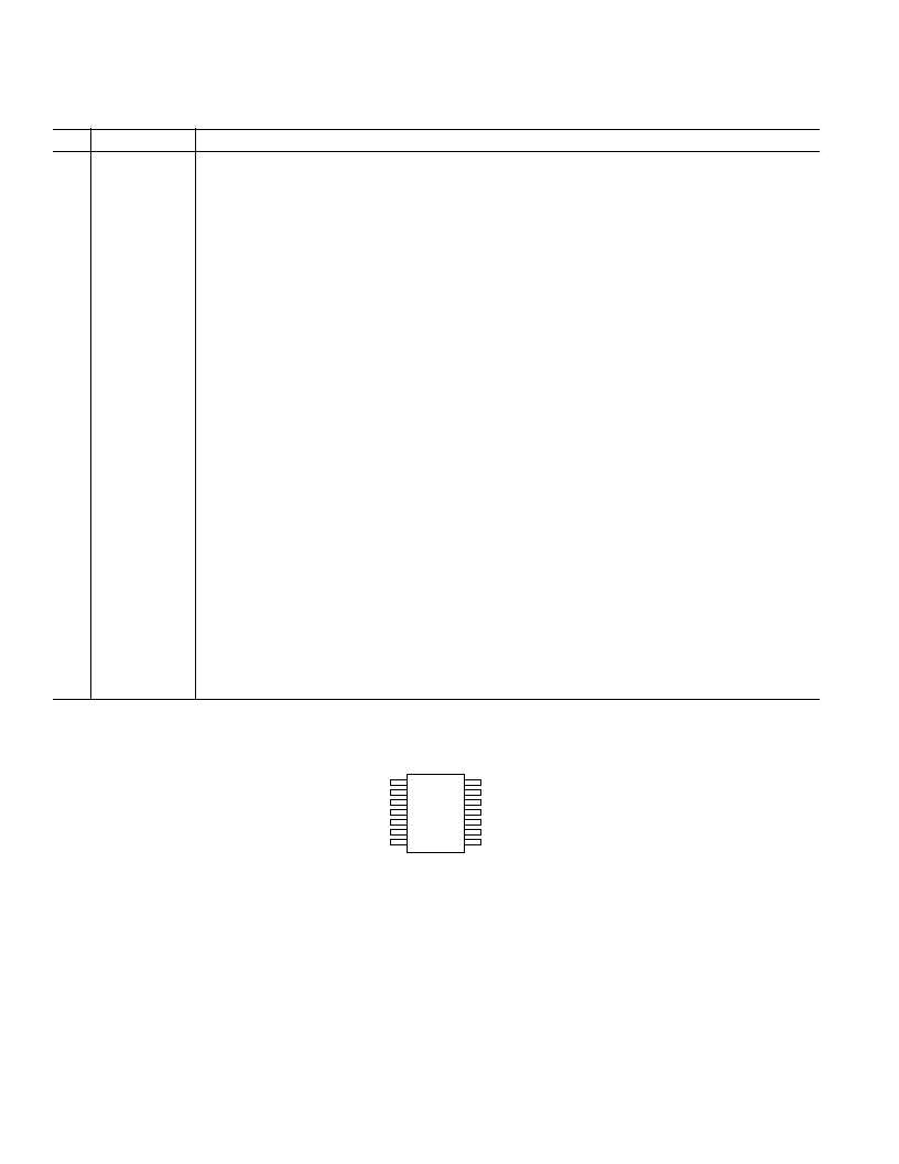
PIN CONFIGURATION
OVPSET
SD
GND
IN
DRVLSD
DLY
VCCGD
BST
DRVH
SW
SRMON
PGND
DRVL
VCC
1
2
3
4
5
6
7
14
13
12
11
10
9
8
ADP3410
相關(guān)PDF資料 |
PDF描述 |
|---|---|
| ADP3410 | Dual MOSFET Driver with Bootstrapping |
| ADP3412 | Replaced by BQ29415 : Voltage Protection for 2, 3, or 4 Cell LiIon Batteries (2nd Lev Protection) 8-SM8 -25 to 85 |
| ADP3412JR | Secondary Over-Voltage Protection for 2-4 cell in series Li-Ion/Poly (4.35V) 8-SM8 -40 to 110 |
| ADP3413 | Secondary Over-Voltage Protection for 2-4 cell in series Li-Ion/Poly (4.35V) 8-SM8 -40 to 110 |
| ADP3413JR | Secondary Over-Voltage Protection for 2-4 cell in series Li-Ion/Poly (4.35V) 8-SM8 -40 to 110 |
相關(guān)代理商/技術(shù)參數(shù) |
參數(shù)描述 |
|---|---|
| ADP3410KRU-REEL | 功能描述:IC MOSFET DVR DUAL N-CH 14TSSOP RoHS:否 類別:集成電路 (IC) >> PMIC - MOSFET,電橋驅(qū)動(dòng)器 - 外部開(kāi)關(guān) 系列:- 標(biāo)準(zhǔn)包裝:50 系列:- 配置:高端 輸入類型:非反相 延遲時(shí)間:200ns 電流 - 峰:250mA 配置數(shù):1 輸出數(shù):1 高端電壓 - 最大(自引導(dǎo)啟動(dòng)):600V 電源電壓:12 V ~ 20 V 工作溫度:-40°C ~ 125°C 安裝類型:通孔 封裝/外殼:8-DIP(0.300",7.62mm) 供應(yīng)商設(shè)備封裝:8-DIP 包裝:管件 其它名稱:*IR2127 |
| ADP3410KRU-REEL7 | 功能描述:IC MOSFET DVR DUAL N-CH 14TSSOP RoHS:否 類別:集成電路 (IC) >> PMIC - MOSFET,電橋驅(qū)動(dòng)器 - 外部開(kāi)關(guān) 系列:- 標(biāo)準(zhǔn)包裝:50 系列:- 配置:高端 輸入類型:非反相 延遲時(shí)間:200ns 電流 - 峰:250mA 配置數(shù):1 輸出數(shù):1 高端電壓 - 最大(自引導(dǎo)啟動(dòng)):600V 電源電壓:12 V ~ 20 V 工作溫度:-40°C ~ 125°C 安裝類型:通孔 封裝/外殼:8-DIP(0.300",7.62mm) 供應(yīng)商設(shè)備封裝:8-DIP 包裝:管件 其它名稱:*IR2127 |
| ADP3412 | 制造商:AD 制造商全稱:Analog Devices 功能描述:Dual MOSFET Driver with Bootstrapping |
| ADP3412JR | 功能描述:IC MOSFET DVR DUAL N-CH 8-SOIC RoHS:否 類別:集成電路 (IC) >> PMIC - MOSFET,電橋驅(qū)動(dòng)器 - 外部開(kāi)關(guān) 系列:- 標(biāo)準(zhǔn)包裝:50 系列:- 配置:高端 輸入類型:非反相 延遲時(shí)間:200ns 電流 - 峰:250mA 配置數(shù):1 輸出數(shù):1 高端電壓 - 最大(自引導(dǎo)啟動(dòng)):600V 電源電壓:12 V ~ 20 V 工作溫度:-40°C ~ 125°C 安裝類型:通孔 封裝/外殼:8-DIP(0.300",7.62mm) 供應(yīng)商設(shè)備封裝:8-DIP 包裝:管件 其它名稱:*IR2127 |
| ADP3412JR-REEL | 制造商:Rochester Electronics LLC 功能描述:HIGH CURRENT DUAL MOSFET DRIVER - Tape and Reel |
發(fā)布緊急采購(gòu),3分鐘左右您將得到回復(fù)。