- 您現在的位置:買賣IC網 > PDF目錄374022 > ADP3422JRU (ANALOG DEVICES INC) Secondary Over-Voltage Protection for 2-4 cell in series Li-Ion/Poly (4.40V) 8-SM8 -40 to 110 PDF資料下載
參數資料
| 型號: | ADP3422JRU |
| 廠商: | ANALOG DEVICES INC |
| 元件分類: | 電源管理 |
| 英文描述: | Secondary Over-Voltage Protection for 2-4 cell in series Li-Ion/Poly (4.40V) 8-SM8 -40 to 110 |
| 中文描述: | 5-CHANNEL POWER SUPPLY SUPPORT CKT, PDSO28 |
| 封裝: | TSSOP-28 |
| 文件頁數: | 14/16頁 |
| 文件大小: | 174K |
| 代理商: | ADP3422JRU |
REV. 0
ADP3422
–14–
6. An external
“
antiparallel
”
schottky diode (across the bottom
MOSFET) may help efficiency a small amount (< ~1 %); a
MOSFET with a built in antiparallel schottky is more effec-
tive. For an external schottky, it should be placed next to
the bottom MOSFET or it may not be effective at all. Also,
a higher current rating (bigger device with lower voltage
drop) is more effective.
7. The ground pin of the ADP3415 should be connected into
the power switching circuitry ground plane, and the VCC
bypass capacitor should be close to the VCC pin and con-
nected into the same ground plane.
Output Filter
Output Inductor and Capacitors, Current Sense Resistor
8. Locate the current sense resistor very near to the output
capacitors.
9. PCB trace resistances from the current sense resistor to the
output capacitors, and from the output capacitors to the
load should be minimized, known (calculated or measured),
and compensated for as part of the design if it is significant.
(Remote sensing is not sufficient for relieving this require-
ment!) A square section of 1-ounce copper trace has a
resistance of ~500 mW. Using 2~3 squares of copper can
make a noticeable impact on a 15 A design.
10. Whenever high currents must be routed between PCB layers,
vias should be used liberally to create several parallel current
paths so that the resistance and inductance introduced by
these current paths is minimized and the via current rating is
not exceeded.
11. The ground connection of the output capacitors should be
close to the ground connection of the lower MOSFET and
it should be a ground plane. Current may pulsate in this
path if the power source ground is closer to the output
capacitors than the power switching circuitry, so a close
connection will minimize the voltage drop.
Control Circuitry
ADP3422, Control Components
12. If the placement overview cannot be followed, then in order
to avoid introducing ground noise from the power switching
stage into the control circuitry, the ground pin of the
ADP3422 should be Kelvin-connected into the ground plane
near the output capacitors. All other control components
should be grounded on that same signal ground.
13. If critical signal lines (i.e., signals from the current sense
resistor leading back to the ADP3422) must cross through
power circuitry, it is best if a signal ground plane can be
interposed between those signal lines and the traces of the
power circuitry. This serves as a shield to minimize noise
injection into the signals at the expense of making signal
ground a bit noisier.
14. Absolutely avoid crossing any signal lines over the switching
power path loop, described previously.
15. Accurate voltage positioning depends on accurate current
sensing, so the control signals which monitor the voltage
differentially across the current sense resistor should be
kelvin connected.
16. The RC filter used for the current sense signal should be
located near the control components.
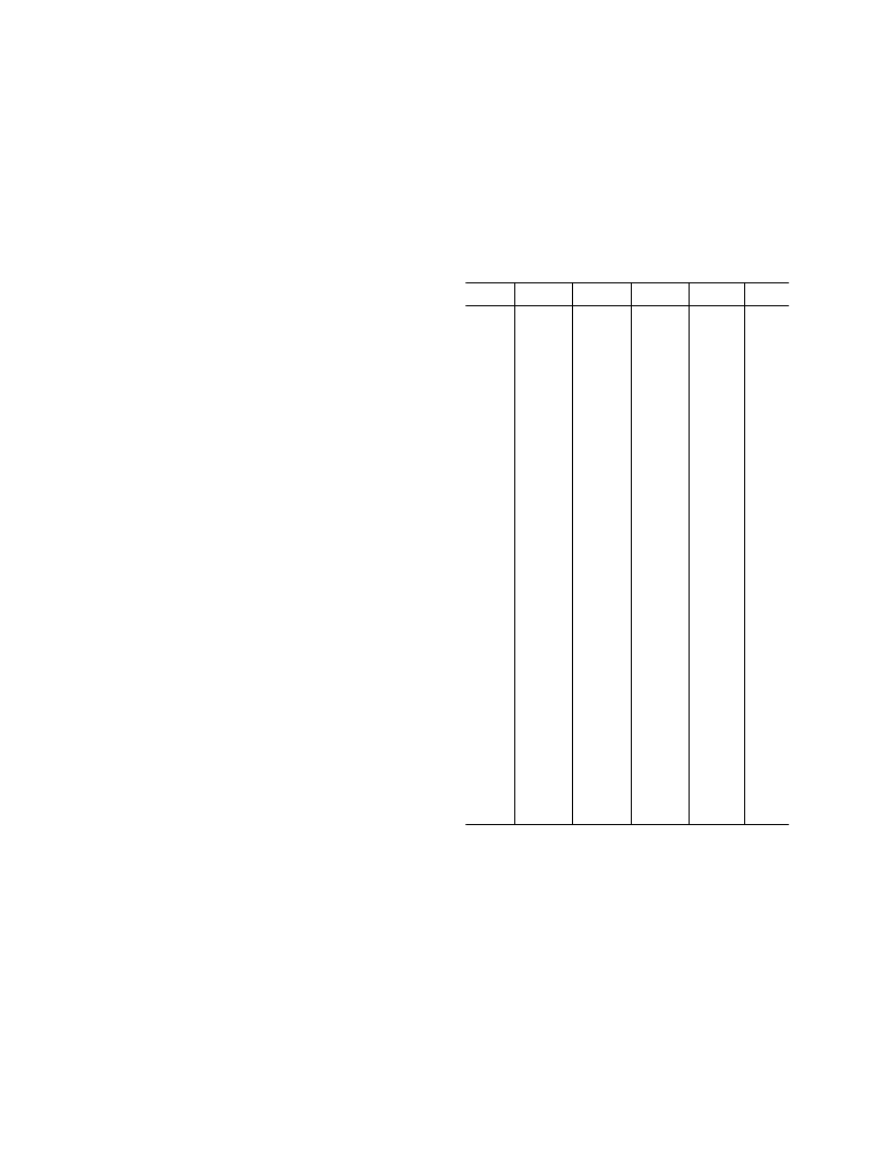
Table I. VID Code
VID4
VID3
VID2
VID1
VID0
V
VID
1.750
1.700
1.650
1.600
1.550
1.500
1.450
1.400
1.350
1.300
1.250
1.200
1.150
1.100
1.050
1.000
0.975
0.950
0.925
0.900
0.875
0.850
0.825
0.800
0.775
0.750
0.725
0.700
0.675
0.650
0.625
0.600
0
0
0
0
0
0
0
0
0
0
0
0
0
0
0
0
1
1
1
1
1
1
1
1
1
1
1
1
1
1
1
1
0
0
0
0
0
0
0
0
1
1
1
1
1
1
1
1
0
0
0
0
0
0
0
0
1
1
1
1
1
1
1
1
0
0
0
0
1
1
1
1
0
0
0
0
1
1
1
1
0
0
0
0
1
1
1
1
0
0
0
0
1
1
1
1
0
0
1
1
0
0
1
1
0
0
1
1
0
0
1
1
0
0
1
1
0
0
1
1
0
0
1
1
0
0
1
1
0
1
0
1
0
1
0
1
0
1
0
1
0
1
0
1
0
1
0
1
0
1
0
1
0
1
0
1
0
1
0
1
相關PDF資料 |
PDF描述 |
|---|---|
| ADP3502 | CDMA Power Management System |
| ADP3502ASU | CDMA Power Management System |
| ADP3510 | Secondary Over-Voltage Protection for 2-4 cell in series Li-Ion/Poly (4.40V) 8-SM8 -40 to 110 |
| ADP3510ARU | Secondary Over-Voltage Protection for 2-4 cell in series Li-Ion/Poly (4.40V) 8-SM8 -40 to 110 |
| ADP3522 | GSM Power Management System |
相關代理商/技術參數 |
參數描述 |
|---|---|
| ADP3422JRU-REEL | 制造商:Analog Devices 功能描述: |
| ADP3430JCPZ-RL | 制造商:ON Semiconductor 功能描述: |
| ADP3500 | 制造商:未知廠家 制造商全稱:未知廠家 功能描述:CDMA Power Management System |
| ADP3500AST | 制造商:未知廠家 制造商全稱:未知廠家 功能描述:CDMA Power Management System |
| ADP3501AST-REEL | 制造商:Analog Devices 功能描述: |
發布緊急采購,3分鐘左右您將得到回復。